
2um - 300um Technical Ceramic Parts Silicon On Insulator SOI Wafer
|


|
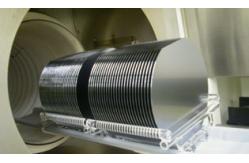
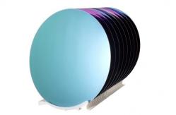
SOI Wafer ( Silicon-on-Insulator )
We provides high quality SOI wafer ( Silicon-on-Insulator ) for a varity of application including MEMS , Power device , Pressure sensors and CMOS integrated circuit fabrication . SOI wafer provide a potential solution for high speed and low power consumption device and has been widely acknowledged as a new solution for high voltage and RF components. SOI wafer is a sandwich structure including a device layer ( active layer ) on top , a buried oxide layer ( insulating SiO2 layer ) in the middle , and a handle wafer ( bulk silicon ) in the bottom . SOI wafers are produced by using SIMOX and wafer bonding technology to achieve thinner and precise device layer and ensure the requirement of thickness uniformity and low defect density . We can provide SOI wafer in diameter 4" and 8 " with flexible thickness and wide resistivity range to meet your unique SOI requirements . Contact us for further SOI product informations .
SOI Wafer Application
Product Specification
|
||||||||||||||||||||||||||||||||||
| Product Tags: SOI Wafer Technical Ceramic Parts 2um SOI Wafer 300um SOI Wafer |
|
High Concentration Quantum Grade Diamond Customized Size |
|
Single Crystal Diamond Cutting Tools Good Wear Resistance |
|
Indusatial Ceramics Parts Cultured Diamonds Pink Blue Yellow |
|
Diamond Heat Dissipation Material Thermal Management For Electronic Packaging Heat Dissipation |
|
Corseed Electrically Conductive Ceramics Handling Arm |
|
High Performance Nozzle Or Injector Technical Ceramic Parts |