
Lead Free 0.3oz Surface Mount PCB Assembly
|


FR-4 Multilayer Surface Mount Lead Free PCB AssemblyLead Free PCB Assembly Introduction
The lead free PCB assembly manufacturing primarily comes in lead-free solder technology and lead-free components and materials.
The RoHS PCB assembly process requires that none of the hazardous materials listed in the RoHS Directive are used in the boards, components or solders. Bare printed circuit boards used in the typical "leaded process" are often coated with a lead-tin finish, so the finish on the board must be modified significantly to be compliant with lead-free and RoHS standards.
Factory Capabilities
PCBA CAPABILITIES
Lead free PCB Aassembly Production Process
PCB,Component sourcing ,QC ,SMT Process ,AOI ,Test ,Automatic optical inspection ,DIP Process ,Washing board ,FQC .
Our WorkShop
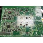
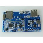
Products Show
PCB Assembly Application Field
Printed circuit boards And PCB Assembly are mainly used for many communication industry : Aerospace ; Telecom Communication ;Military & ; Automotive Industry ;Industrial Control ;Consumer Electronics ,
Delivery Time
Partners
Common packaging
FAQ
Q1:What kind of PCB file format can you accept for production?
Q2:Is my PCB files safe when I submit them to you for manufacturing? We respect customer's copyright and will never manufacture PCB for someone else with your files unless we receive written permission from you, nor we'll share these files with any other 3rd parties.
Q3:What payments do you accept ?
Q4:How to get the PCB?
Q5:What is your minimum order quantity?
Q6: Can we visit your company? No problem. You are welcome to visit us in Beijing. Or the branch factory is in Tianjin.
Q7: How can you ensure the quality of the PCB?
|
||||||||||||||||||||||||||||||||||||||||||||||||||||||||||||||||||||||||||||||||||||||||||||||||||||||||||||||||||||||||||||||||||||||||||||||||||||
| Product Tags: OEM surface mount PCB assembly 0.3oz surface mount PCB assembly RoHS Printed Circuit Board Assembly PCBA | ||||||||||||||||||||||||||||||||||||||||||||||||||||||||||||||||||||||||||||||||||||||||||||||||||||||||||||||||||||||||||||||||||||||||||||||||||||
|
100% Lead Free Prototype Pcb Assembly Solder Paste Multi-Layer |

|
4 Layers Rohs Lead Free Pcb Assembly Compliance Surface Mount Technology |

|
6 Layers Hdi 1oz Medical Pcb Assembly Bga 0.18mm 3/3 Mil Trace |

|
Enig Finger Gold Fr 4 Pcb Assembly 8 Layer Hasl |

|
Multilayer Lead Free Pcb Assembly Buried Blind Hole Plate Dip Hasl |
|
1oz Rigid Cem-1 Turnkey Pcb Assembly Hasl One Stop Service |