
2 Layer Pcb Smt Assembly Fr4 Hasl Qfn Bga Dip Impedance Control
|


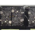
FR4 HASL QFN BGA DIP Impedance Control Pcb SMT Assembly
PCB SMT Assembly IntroductionOur Service: Full Turnkey PCB Assembly; PCB Assembly Services; Lead-free Assembly; PCB Assembly Quote; Prototype PCB Assembly; BGA Assembly; Components Sourcing Service; Panel Requirements for Assembly; Surface Mount (SMT) PCB Assembly; Functional Testing; HDI PCB Assembly; Box Assembly
PCBA CAPABILITIES
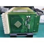
PCB assembly process
PCB: Drilling--Exposure--Plating--Etaching & Stripping--Punching--Electrical Testing--SMT--Wave Soldering--Assembling--ICT--Function Testing--Temperature & Humidity Testing PCBA : 1.Solder Paste stenciling---2.Surface Mount Technology (Pick and Place)---3.Reflow Soldering---4.Inspection and Quality Control---5.Through-Hole Component Insertion (DIP Process)---6.Final Inspection and Functional Test
Our advantage
1.Service value Independent quotation system to quickly serve the market 2.PCB manufacturing High-tech PCB and PCB assembly production line 3.Material purchasing A team of experienced electronic component procurement engineers 4.SMT post soldering Dust-free workshop, high-end SMT patch processing
PCB SMT Assembly Delivery Time
Electronic Board Assembly Application Field
Our products are widely used in communication equipment, industrial control, consumer electronics, medical equipment, aerospace, light-emitting diode lighting, automotive electronics etc.
Workshop
Common packaging
1.PCB: Vacuum packaging with carton box
FAQ:
Q1:What service do you have? A1: We provide turnkey solution including RD, PCB fabrication, SMT,
final assembly,testing and other Q2:What are the main products of your PCB/PCBA services? A2:Our PCB/PCBA services are mainly for the industries including
Medical, Automotive, Energy, Q3:How can we ensure our information should not let third party to see our design? A3: We are wiling to sign NDA effect by customer side locallaw and promising to keep customers datain highconfidential level. Q4:What does Parason need for a customized PCB order? A4:When you place a PCB order, the customers need to provide Gerber or pcb file.If you do not have the fileinthe correct format, you can send all the details related to the products. Q5:What will be needed for a customized PCBA order? A5: When you place a PCBA order, you need to provide Gerber or pcb file and the BOM list to us. Q6:Do you have an minimum order quantity? A6:We accept order with as low as a quantity of 1 (piece or panel)
|
||||||||||||||||||||||||||||||||||||||||||||||||||||||||||||||||||||||||||||||||||||||||||||||||||||||||||||||||||||||||||||||||||||||||||||||||
| Product Tags: 2 layer smt pcb assembly pcb smt assembly fr4 2 layer pcb smt assembly | ||||||||||||||||||||||||||||||||||||||||||||||||||||||||||||||||||||||||||||||||||||||||||||||||||||||||||||||||||||||||||||||||||||||||||||||||

|
Fr4 Quick Turn Clean Vacuum Pcb Smt Assembly Printed Circiut Board Design |

|
1oz Hasl Dual In Line Package Dip Smt Pcb Assembly Fr-4 |

|
Hasl 94vo Qfn Bga Dip Rigid Fr4 Pcb Assembly |
|
2 Layer Pcb Smt Assembly Fr4 Hasl Qfn Bga Dip Impedance Control |

|
1/3oz Hasl Lead Free Smt Pcba Black Solder Mask Color |
|
Fr4-Standard Tg 1 30-140c Surface Mount Pcb Assembly Green For Video Processing Technology |