
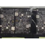
Oem Hdi Pcb Assembly 1.6mm Smt For Communication Equipment
|


OEM HDI 1.6mm PCB SMT Assembly
PCBA Manufacturer IntroductionWe are One Professinal Mid-to-High-End PCB and PCB Assembly
solutions provider . Our PCBAs Mainly used in Military-Industrial sphere ,Automotive
/automobile , Medical .Communication Solution, Industrial Control,
Aerospace , image processing ,video processing technology ,smart
home ,securit etc. PCB CAPABILITIES
Assembly Types: Surface mount, Thro-hole, Mixed technology (SMT & Thru-hole), Single or double sided placement, Conformal coating, Shield cover assembly for EMI emission control
PCBA CAPABILITIES
Our advantage
Service value Independent quotation system to quickly serve the market
PCB manufacturing High-tech PCB and PCB assembly production line
Material purchasing A team of experienced electronic component procurement engineers
SMT post soldering Dust-free workshop, high-end SMT patch processing
Why choose us?
Welcome to visit our factory, Haina lean Electronics Co., Ltd.
Delivery Time
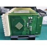
PCBA Manufacturer Application Field
Our products are widey used in many communication industry, power, security, optoelectronics, industrial control, medical equipments, consumer electronics and automobile industry etc field.
Workshop
Partners
Common packaging
Certification
FAQ
FAQ Q1.What are needed for quotation? Q2. What file formats do you accept for production? Q3.Are my files safe? Q4.MOQ? Q5.Shipping Cost ? The shipping cost is determined by the destination ,weight ,packing size of the goods .We can provide shipping, air, land, express and other transportation services . Q6.How to ensure high-quality production? Q7.What are the services you can provide ? One-stop contract manufacturing Yes , we will test each piece of PCBA product under your testing methods ,to ensure quality and functionality . Q9.Do you provide OEM service ? Yes ,we offer PCB and PCBA OEM/ODM Service , produce the PCB and PCBA products as your design and requirements .
Company Information
Haina lean Electronics Co., Ltd is a one-stop EMS supplier integrating PCB design, PCB manufacturing, Component sourcing and PCB assembly. Our company was established in May 1, 2012 in Beijing. And expansion was completed in June 2016. The company is specialized in electronic products supporting processing services, mainly to undertake circuit board design, layout production, components procurement, PCB plate making, circuit board welding assembly debugging and other OEM/ODM services.
At present, the main cooperation industries are automotive electronics, communications, audio and video, optoelectronics, robotics, hydroelectric power, medical care, aerospace, education, radio frequency, power supply, printer etc industries.
|
||||||||||||||||||||||||||||||||||||||||||||||||||||||||||||||||||||||||||||||||||||||||||||||||||||||||||||||||||||||||||||||||||||||||||||||||||||
| Product Tags: oem hdi pcb assembly smt hdi pcb assembly pcb smt assembly 1.6mm | ||||||||||||||||||||||||||||||||||||||||||||||||||||||||||||||||||||||||||||||||||||||||||||||||||||||||||||||||||||||||||||||||||||||||||||||||||||

|
Fr4 Quick Turn Clean Vacuum Pcb Smt Assembly Printed Circiut Board Design |

|
1oz Hasl Dual In Line Package Dip Smt Pcb Assembly Fr-4 |

|
Hasl 94vo Qfn Bga Dip Rigid Fr4 Pcb Assembly |
|
2 Layer Pcb Smt Assembly Fr4 Hasl Qfn Bga Dip Impedance Control |

|
1/3oz Hasl Lead Free Smt Pcba Black Solder Mask Color |
|
Fr4-Standard Tg 1 30-140c Surface Mount Pcb Assembly Green For Video Processing Technology |