
Low Dk Multilayer HDI Lead Free PCB Assembly
|


Low Dk Multilayer HDI Lead Free PCB AssemblyLead Free PCB Assembly Introduction
We have a comprehensive lead-free solder solution. including solder
alloy selection, solder paste evaluation, wave solder flux
evaluation, process optimization, design rules, components
evaluation, reliability, equipment evaluation, quality inspection
and production costs. We have worked actively with industry
standard organizations to facilitate the industry-wide transition
to lead-free products.
Factory Capabilities
PCBA CAPABILITIES
PCB Aassembly Production Process
PCB,Component sourcing ,QC ,SMT Process ,AOI ,Test ,Automatic optical inspection ,DIP Process ,Washing board ,FQC .
Our WorkShop
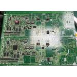
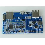
Products Show
PCB Assembly Application Field
Printed circuit boards And PCB Assembly are mainly used for many communication industry : Aerospace ; Telecom Communication ;Military & ; Automotive Industry ;Industrial Control ;Consumer Electronics .etc.
Delivery Time
Partners
Common packaging
FAQ
Q1.What are needed for quoation ? PCB :Gerber File (Protel.Power PCB ,PADs File)
Q2.What file formats do you accept for production ? Gerber file :CAM350 RS274X
Q3.Are my files safe ? Your files are held in complete safety and security ,we protect the intellectual property for our customers in the whole process .All documents from customer are never shared with any third parties .
Q4.What's your MOQ ? No Moq ,We accept small orders as well as mass production
Q5.Shipping Cost ? The shipping cost is determined by the destination ,weight ,packing size of the goods .We can provide shipping, air, land, express and other transportation services .
Q6.Can You provide fast rotating PCB ? Yes , we can provide fast service 24 hours .
Q7.What are the services you can provide ? One-stop contract manufacturing
Yes , we will test each piece of PCBA product under your testing methods ,to ensure quality and functionality .
Q9.Do you provide OEM service ? Yes ,we offer PCB and PCBA OEM Service , we manufacture the PCB and PCBA products to your design and requirements . |
||||||||||||||||||||||||||||||||||||||||||||||||||||||||||||||||||||||||||||||||||||||||||||||||||||||||||||||||||||||||||||||||||||||||||||||||||||
| Product Tags: Low Dk Lead Free PCB Assembly HDI Lead Free PCB Assembly Multilayer HDI PCB Assembly | ||||||||||||||||||||||||||||||||||||||||||||||||||||||||||||||||||||||||||||||||||||||||||||||||||||||||||||||||||||||||||||||||||||||||||||||||||||
|
100% Lead Free Prototype Pcb Assembly Solder Paste Multi-Layer |

|
4 Layers Rohs Lead Free Pcb Assembly Compliance Surface Mount Technology |

|
6 Layers Hdi 1oz Medical Pcb Assembly Bga 0.18mm 3/3 Mil Trace |

|
Enig Finger Gold Fr 4 Pcb Assembly 8 Layer Hasl |

|
Multilayer Lead Free Pcb Assembly Buried Blind Hole Plate Dip Hasl |
|
1oz Rigid Cem-1 Turnkey Pcb Assembly Hasl One Stop Service |