
2-layer TP1600 High-DK PCB 0.9mm Thick Pure Gold Finish
|
|
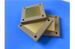
This rigid 2-layer TP1600 high-Dk RF PCB is fabricated with specialized ceramic-filled PPO resin dielectric laminate, featuring an ultra-high dielectric constant of 16.0 for circuit miniaturization. Adopting pure gold plating surface finish and manufactured in compliance with IPC-Class-2 industrial standards, this 0.9mm thick PCB delivers stable low dissipation factor, precise dielectric control and radiation resistance. Without fiberglass reinforcement, TP1600 eliminates the weave effect for consistent electrical performance. It is highly suitable for miniaturized antennas, microwave filters, aerospace payloads and defense navigation systems.
PCB Specifications
PCB Stack-up Configuration
Artwork Format & Compliance Standard Artwork Format: Delivered in Gerber RS-274-X, the universal industrial standard ensuring high-precision PCB fabrication and full data compatibility.
Accepted Standard: IPC-Class-2, ensuring stable and long-term service performance for industrial and military high-frequency electronic devices.
Availability: Global shipping service is provided to support worldwide engineering procurement and industrial projects.
Introduction of TP1600 Substrate TP1600 is a specialized high-frequency microwave composite dielectric copper-clad laminate (CCL) belonging to the TP material series. Adopting ceramic-filled polyphenylene oxide (PPO) resin matrix without fiberglass reinforcement, this substrate is molded through high-precision compression technology. The naming convention indicates its fixed nominal dielectric constant of 16.0, which is precisely tuned by adjusting the mixing ratio of ceramic powder and PPO resin.
With exclusive customized production craftsmanship, TP1600 delivers excellent dielectric repeatability and industrial-grade reliability. The fiberglass-free structure eliminates weave effect interference, achieving uniform electrical distribution across the entire board. This high-Dk substrate is widely trusted for military, aerospace and high-precision microwave electronic systems.
Key Features TP1600 integrates superior electrical, mechanical and environmental properties for high-Dk microwave industrial applications:
Material Type: Fiberglass-free ceramic-filled PPO resin copper-clad laminate
Dielectric Constant: 16.0 ± 0.32, enabling extreme circuit miniaturization for compact antennas
Dissipation Factor: 0.0012, maintaining ultra-low signal loss up to 10 GHz
Temperature Coefficient of Dk (TcDk): -43ppm/°C for stable dielectric performance under temperature fluctuation
Z-axis CTE: 45ppm/°C, effectively reducing thermal expansion deformation
Smooth substrate surface without fiberglass weave effect
Radiation resistance & low outgassing for harsh aerospace environments
Key Benefits TP1600 provides irreplaceable technical advantages for high-Dk microwave circuit designers:
Ultra-high Dk value supports miniaturized antenna and resonant structure design to save board space
Extremely low Df ensures minimal signal attenuation for high-frequency matching networks
Fiberglass-free construction avoids signal distortion caused by weave effect
Excellent radiation resistance adapts to aerospace, satellite and military working conditions
Easier machining than pure ceramic substrates with higher production yield and lower cost
Reliable copper adhesion prevents delamination during precision processing
Typical Applications This TP1600 2-layer RF PCB is extensively applied in high-Dk precision microwave and defense electronic equipment:
-Miniaturized Antennas & High-Frequency Sensor Modules -RF/Microwave Filters, Couplers and Resonant Cavities -Aerospace, Defense and Satellite Payload Systems -Beidou Navigation and Missile-Borne Fuze Electronic Units
|
||||||||||||||||||||||||||||||||||
| Product Tags: high frequency copper clad laminate F4BM245 copper clad sheet laminated copper sheet PCB |

|
2-Layer WL-CT350 4mil Ultra--thin PCB Laminate with Immersion Gold Finish |

|
Double-sided 7.5mil TLY-5 Material Ultra-Low Loss Millimeter Wave PCB |
|
2-Layer TFA300 PCB on 5mil High-Frequency Substrate |

|
Copper Coin Embedded PCB 6-Layer M6+High TG FR4 |

|
Double-Sided CER-10 High-Frequency PCB 30mil Laminate Immersion Silver |

|
2-layer TFA294 PCB Low-loss Microwave Circuits with Immersion Gold |