
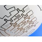
10mil RT duroid 5880 PCB Dual Layer Copper Filled Via
|

|
Introduction to RT/duroid 5880
Key Features
Dielectric Constant: A consistent value of 2.2, with a tight
tolerance of 0.02 at 10 GHz / 23°C, ensures reliable signal
propagation. Dissipation Factor: An exceptionally low dissipation factor of
0.0009 at 10 GHz minimizes energy loss, enhancing the efficiency of
high-frequency circuits. Temperature Coefficient of Dielectric Constant (TCDk): With a TCDk
of -125 ppm/°C, the PCB maintains stable performance across a range
of temperatures. Moisture Absorption: A low moisture absorption rate of just 0.02%
makes this PCB ideal for high-moisture environments, preventing
degradation over time. Isotropic Properties: The PCB exhibits isotropic behavior, with a coefficient of thermal expansion (CTE) of 31 ppm/°C along the X-axis, 48 ppm/°C along the Y-axis, and 237 ppm/°C along the Z-axis.
Benefits
Uniform Electrical Properties: Consistent electrical performance is
achieved across a wide frequency range, ensuring reliability in
demanding applications. Machinability: The material can be easily cut, sheared, and
machined, allowing for flexibility in design and manufacturing
processes. Chemical Resistance: Resistance to solvents and reagents typically
used in PCB fabrication enhances durability and longevity. Ideal for Moist Environments: The low moisture absorption rate
makes it suitable for applications in high-humidity settings, where
other materials may fail. Proven Reliability: Recognized as a well-established material, RT/duroid 5880 is known for its low electrical loss among reinforced PTFE materials.
PCB Construction and Specifications
Stackup: The PCB features two copper layers (35 μm each)
encompassing a core of RT/duroid 5880 that measures 0.254 mm (10
mil). Board Dimensions: The dimensions are set at 50 mm x 45 mm, with a
tolerance of ±0.15 mm, facilitating integration into various
designs. Minimum Trace/Space: A minimum trace and space of 5/4 mils allows
for high-density designs without compromising performance. Minimum Hole Size: A minimum hole size of 0.2 mm supports a variety
of component footprints. Finished Thickness: The finished board thickness is 0.4 mm, with an
outer copper weight of 1 oz (1.4 mils). Surface Finish: Immersion gold is applied, ensuring excellent
electrical performance and protection against environmental
factors. Silkscreen and Solder Mask: The top silkscreen is printed in white,
while the top solder mask is matte green; no bottom silkscreen or
solder mask is included. Vias: The PCB includes a total of 42 vias, with copper filling on
designated IC pads. Testing: A rigorous 100% electrical testing is conducted prior to shipment to ensure functionality and reliability.
Quality Assurance
Typical Applications
Commercial Airline Broadband Antennas
The RT/duroid 5880 2-Layer Rigid PCB is positioned as a high-performance, reliable solution designed to meet the rigorous demands of modern electronic applications.
|
|||||||||||||||||||||||||||||||||||||||||||||||||||||||||||||||||||||||||||||||||||||||||||||||||||||||||||||||||||||||||||||||||||||||||||||||||||||||||||||||||||||||||||||||||||||
| Product Tags: 10mil RT duroid 5880 PCB Dual Layer RT duroid 5880 PCB | |||||||||||||||||||||||||||||||||||||||||||||||||||||||||||||||||||||||||||||||||||||||||||||||||||||||||||||||||||||||||||||||||||||||||||||||||||||||||||||||||||||||||||||||||||||

|
2-Layer TFA294 PCB 80mil Laminate Circuit Board OSP Finish |

|
0.8mm TP2500 Substrate 2-layer RF PCB Pure Gold Plating |
|
25mil TF300 Laminate 2L High Frequency PCB ENEPIG Finish |

|
Double-Sided TP960 PCB 1mm Core Substrate EPIG Finish |

|
Double-layer TF440 PCB 0.7mm Ultra-Low Loss Immersion Gold Finish |

|
10.9mm Wangling TP2200 Double-Layer High Frequency PCB High Dk Circuit Board |