
Copper 1oz Impedance Controlled PCB 8 Layer For Wireless HDMI
|
Detailed Product Description
|
Impedance Controlled PCB Differential Impedance Circuit Board 8
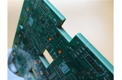
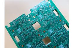
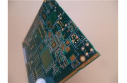
Layer PCB for Wireless HDMI 1.1 General description This is a type of 8 layer printed circuit board built on FR-4
substrate with Tg 170°C for the application of Wireless HDMI. It's
1.6 mm thick with white silkscreen(Taiyo) on green solder mask
(Taiyo) and immersion gold on pads. It's also an impedance
controlled PCB with single-end impedance and differential impedance
controlled on on top layer and bottom layer. The base material is
from Taiwan ITEQ supplying 1 up PCB per panel. They're fabricated
per IPC 6012 Class 2 using supplied Gerber data. Each 25 panels are
packed for shipment. 1.2 Features and benifits Lead free assemblies with a maximum reflow temperature of 260℃ High solderability, no stressing of circuit boards and less
contamination of PCB surface. AOI inspection 8000 types of PCB per month 12 hours quotation Free-of-charge PCB panelization 1.3 Applications USB Adapter WiFi USB Dongle GPRS Modem 1.4 Parameter and data sheet
1.5 Characteristic Impedance The characteristic impedance of the conductor on the printed
circuit board is an important indicator of the circuit design,
especially in the PCB design of high frequency circuit. Whether the
characteristic impedance of the conductor is consistent and
matching with the characteristic impedance required by the device
or signal must be taken into consideration. Therefore, these two
concepts in reliability design of PCB design must be paid
attention. There will be a variety of signal transmission in the conductor of
circuit board. To increase the rate of transmission, it must
increase its frequency. Due to the factors of the circuit itself
such as etching, stack thickness, track width and so on are
different, it will cause changes of the impedance value, resulting
in its signal distortion. Therefore, the impedance value of
conductor on high-speed circuit board should be controlled within a
certain range, known as the "impedance control". The factors that
affect the impedance of the PCB wiring are mainly the width of the
copper track, the thickness of the copper track, the dielectric
constant of the dielectric, the thickness of the dielectric, the
thickness of the pad, the path of the ground layer, the wires
around the wiring, etc. So the impedance of the wiring on the board
must be controlled in the design of the PCB to avoid signal
reflection and other electromagnetic interference and signal
integrity issues as far as possible, to guarantee the stability of
the actual use of the PCB board. You can refer to the corresponding
empirical formula for the calculation method of micro-strip line
and strip line impedance on PCB board. |
||||||||||||||||||||||||||||||||||||||||||||||||||||||||||||||||||||||||||||||||||||||||||||
| Product Tags: 1oz Impedance Controlled PCB 8 Layer Impedance Controlled PCB 1oz HDMI Circuit Board |
Related Products

|
TU-768 Lead Free PCB Multilayer Printed Circuit Board glass coated |

|
Keypad PCB Hard Gold Circuit Board Built On Tg170 FR-4 With Green Solder Mask |

|
Immersion Gold Double Sided High Temperature PCB For Automotive |

|
Multi Layer FR4 PCB Board High Tg Lead Free 400mmX500mm |

|
High Tg PCB Printed Circuit Board S1000-2MB Prepreg With Immersion Gold |

|
Multilayer High Tg FR4 PCB Board With 1.2mm Thick Coating Immersion Gold |
Email to this supplier