
11 - 20 of 690
fr4 6 layer hdi pcb
Selling leads

|
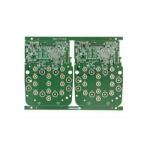
... is the best alternative to high-layer-count and expensive standard laminate or sequentially laminated boards. HDI incorporate blind and buried ...
2024-12-09 17:39:15
|
|
|
... is the best alternative to high-layer-count and expensive standard laminate or sequentially laminated boards. HDI incorporate blind and buried ...
2026-04-21 00:17:11
|
|
...Layer HDI Prinred Circuit Boards FR4 TG170 Green Soldermask High Density HDI PCB Manufacturer Company Profile: Abis Circuits Co., Ltd is a ...
2024-12-09 17:22:10
|
|
|
...Layer HDI Prinred Circuit Boards FR4 TG170 Green Soldermask High Density HDI PCB Manufacturer Company Profile: Abis Circuits Co., Ltd is a ...
2026-04-21 00:17:11
|

|
... Layer Insulation Layer Thickness 0.075mm--5.00mm Min.hole size 0.1mm (drilling hole) Max. Board size 1200mm*600mm Out Layer Copper Thickness 18um-...
2024-12-09 13:35:10
|
|
|
... Layer Insulation Layer Thickness 0.075mm--5.00mm Min.hole size 0.1mm (drilling hole) Max. Board size 1200mm*600mm Out Layer Copper Thickness 18um-...
2024-12-09 18:57:10
|

|
...FR4 94v0 HDI PCB Board PCBA 8.00mm Thickness Abis Circuits Co., Ltd is a professional PCB manufacturer which was established in Oct 2006 and ...
2024-12-09 13:34:21
|
|
|
...FR4 94v0 HDI PCB Board PCBA 8.00mm Thickness Abis Circuits Co., Ltd is a professional PCB manufacturer which was established in Oct 2006 and ...
2026-04-21 00:17:11
|

|
HDI PCB Technology For Telecommunication Industry 1. 12 layer PCB. 2. FR4 High Tg substrate. 3. Blind via,Buried via,VIP process. 4. Telecommunication ...
2024-12-09 13:17:07
|
|
|
HDI PCB Technology For Telecommunication Industry 1. 12 layer PCB. 2. FR4 High Tg substrate. 3. Blind via,Buried via,VIP process. 4. Telecommunication ...
2024-12-09 18:57:10
|