
Main Board Multilayer PCB
|


|
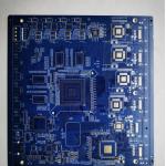
Quick Turn Metering Multi Layer PCB Main Board with HASL Finishing
Abis Circuits Co. Ltd, established in 2006, Located in Shenzhen, our company has about 1100 workers and two PCB workshops with about 50000 square meters.
1. Single, Double side & Multi-layer PCB. 2. Buried/Blind Vias, Via in Pad, Counter Sink Hole, Screw Hole(Counterbore), Press-fit, Half Hole. 3. HASL lead-free, Immersion Gold/ Silver/Tin, OSP, Gold plating/finger, Peelable mask, 4. Printed Circuit Boards adhere to IPC Class 2 & 3 international PCB standard. 5. Quantities range from prototype to medium&big batch production. 6.100% E-Test.
Multiple Quality Assuring Procedures
* Visual Inspection
Monthly Capacity
Lead Time:
How to get a quote?
Please send gerber file with these format: .PCB / .P-CAD / .DXP /
.CAD / .Gerber
FAQ:
Q1: How can I get a quotation:
Q3: Do you have PCB in stock?
Capacility:
Certificates:
ABIS With Customer:
ABIS cares every your order even 1 piece
|
|||||||||||||||||||||||||||||||||||||||||||||||||||||||||||||||||||||||||||||||||||||||||||||||||||||||||||||||||||||||||||||||||||||||||||||||||||||||||||||||||||||||||||||||||||||||||||||||||
| Product Tags: Quick Turn Multi Layer PCB Main Board Multilayer PCB 35um Copper PCB Board | |||||||||||||||||||||||||||||||||||||||||||||||||||||||||||||||||||||||||||||||||||||||||||||||||||||||||||||||||||||||||||||||||||||||||||||||||||||||||||||||||||||||||||||||||||||||||||||||||

|
TG170 14Layer Fr4 PCB Board ENIG Surface Finish Resin plug hole Min hole 0.2 |

|
Resin plug hole 6l board TG170 ENIG PCB Customized Printed Circuit Board |
|
TG170 8 Layer Fr4 PCB Board ENIG Surface Finish Blue Solder Mask Min hole 0.2 |

|
FR4 TG130 Multi Layer PCB ENIG Gold Finger HMT PCB 6 Layers PCB |

|
Customized Multilayer PCB Board Fabrication FR4 Base |

|
HASL Surface Multilayer Printed Circuit Board 1-30 Layers |