
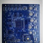
FR4 TG130 Multi Layer PCB ENIG Gold Finger HMT PCB 6 Layers PCB
|


Electronic Board, Rogers PCB, Rogers, High Performance, RF Identification Tags,Multi-LayerAbis Circuits Co. Ltd is a great PCB manufacturer that was established in 2006 and is based in Shenzhen (China’s “Silicon Valley”).
What is the feature of Gold Finger PCB?
A row of golden conductive contacts on the PCB is called "gold fingers". The golden finger (Edge Connector) in the PCB design and production industry uses the plug of the connector as the outlet for the external connection of the board to the network. The main function of the gold finger is to connect, so it must have good electrical conductivity, wear resistance, oxidation resistance, and corrosion resistance.
What certificate does ABIS have?
We have ISO14001, ISO9001, UL, cUL, and TS16949. You can see more in our company profile.
What are the application fields of Circuit boards with Gold Finger? The circuit board can be inserted into or pulled out of the card slot by gold fingers. The application fields of circuit boards are computers' mainboards, game consoles, power circuits, and other high-tech fields.
What capacity does ABIS have?
What is your Lead Time?
We are not only good at product quality but also FINANCIALLY FIT
because we pay attention to goodwill since 2006 in this opening
city-Shenzhen, China.
|
|||||||||||||||||||||||||||||||||||||||||||||||||||||||||||||||||||||||||||||||||||||||||||||||||||||||||||||||||||||||||||||||||||||||||||||||||||||||||||||||||
| Product Tags: FR4 TG130 Multi Layer PCB ENIG Multi Layer PCB Gold Finger 6 layers pcb | |||||||||||||||||||||||||||||||||||||||||||||||||||||||||||||||||||||||||||||||||||||||||||||||||||||||||||||||||||||||||||||||||||||||||||||||||||||||||||||||||

|
TG170 14Layer Fr4 PCB Board ENIG Surface Finish Resin plug hole Min hole 0.2 |

|
Resin plug hole 6l board TG170 ENIG PCB Customized Printed Circuit Board |
|
TG170 8 Layer Fr4 PCB Board ENIG Surface Finish Blue Solder Mask Min hole 0.2 |

|
FR4 TG130 Multi Layer PCB ENIG Gold Finger HMT PCB 6 Layers PCB |

|
Customized Multilayer PCB Board Fabrication FR4 Base |

|
HASL Surface Multilayer Printed Circuit Board 1-30 Layers |