China PCB Assembly Service manufacturer
Chengdu Cesgate Technology Co., Ltd
Work With CESGATE, Work With A Professional And Reliable PCBA Manufacturer
5
Home > Products > Main PCBA >

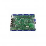
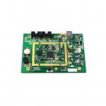
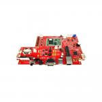
Led Light Main PCBA Customized 3D Printing High Density Interconnect Circuit

Browse Categories

Chengdu Cesgate Technology Co., Ltd

City: chengdu

Province/State:sichuan

Country/Region:china

Tel:86-183-49393344

Contact Person:
Miss.Sia Li
View Contact Details

Led Light Main PCBA Customized 3D Printing High Density Interconnect Circuit

Brand Name CESGATE
Model Number NA
Certification UL, IATF16949, ISO9001
Place of Origin China
Minimum Order Quantity 1PCS( NO MOQ)
Price Negotiable (Depends on your GERBER and BOM)
Payment Terms T/T, L/C
Supply Ability 13kk soldering spot/day
Delivery Time 3-7 working days
Packaging Details PCB: Vacuum Packing / PCBA: ESD Packing
Product name Led Light Main PCBA Customized 3D Printing High Density Interconnect Circuit
Feature Customized 3D printing
High-end equipment FUJI NXT3/XPF laminator
Material FR4/M4/M6/Rogers/TU872/IT968
Lead time 3-7 working days
Test AOI/SPI/XRAY/First Article Inspection
X-ray Supported
Number of I/O IC, SPI, UART/USART
Detailed Product Description

Led Light Main PCBA Customized 3D Printing High Density Interconnect Circuit


Design Procedure of Main PCBA

Manufacturing starts from the fabrication data generated by computer aided design, and component information. The fabrication data is read into the CAM (Computer Aided Manufacturing) software. CAM performs the following functions:

  1. Input of the fabrication data.
  2. Verification of the data
  3. Compensation for deviations in the manufacturing processes (e.g. scaling to compensate for distortions during lamination)
  4. Panelization
  5. Output of the digital tools (copper patterns, drill files, inspection, and others)


Solder resist application in Main PCBA

Areas that should not be soldered may be covered with solder resist (solder mask). The solder mask is what gives main PCBA their characteristic green color, although it is also available in several other colors, such as red, blue, purple, yellow, black and white. One of the most common solder resists used today is called "LPI" (liquid photoimageable solder mask).A photo-sensitive coating is applied to the surface of the PWB, then exposed to light through the solder mask image film, and finally developed where the unexposed areas are washed away. Dry film solder mask is similar to the dry film used to image the PWB for plating or etching. After being laminated to the PWB surface it is imaged and developed as LPI. Once but no longer commonly used, because of its low accuracy and resolution, is to screen print epoxy ink. In addition to repelling solder, solder resist also provides protection from the environment to the copper that would otherwise be exposed.


Specification


NO.ItemsCapabilities
1Layers2-68L
2Maximum machining size600mm*1200mm
3Board thickness0.2mm-6.5mm
4Copper thickness0.5oz-28oz
5Min trace/space2.0mil/2.0mil
6Minimum finished aperture0. 10mm
7Maximum thickness to diameter ratio15:1
8Via treatmentVia, blind&buried via, via in pad, Copper in via …
9Surface finish/treatmentHASL/HASL lead free, Chemical tin, Chemical Gold, Immersion gold Inmersion Silver/Gold, Osp, Gold Plating
10Base MaterialFR408 FR408HR, PCL-370HR;IT180A, Megtron 6(Panasonic);Rogers4350,
Rogers4003, RO3003, Rogers/Taconic/Arlon/Nelco laminate with FR-4 material(including partial Ro4350B hybrid laminating with FR-4)
11Solder mask colorGreen.Black.Red.Yellow.White.Blue.Purple.Matte Green. Matte Black
12Testing ServiceAOI, X-Ray, Flying-Probe, Function Test, First Article Tester
13Profiling PunchingRouting,V-CUT,Beveling
14Bow&twist≤0.5%
15HDI type1+n+1,2+n+2,3+n+3
16Min mechanical aperture0.1mm
17Min laser aperture0.075mm


Advantages of CESGATE:


1. Professional component certification engineer
2. Perfect IQC inspection system
3. Assist in improving customer BOM accuracy

4. Solve the problem of R&D samples
5. Professional supply chain team support
6. R&D procurement can also enjoy VIP customer service

FAQ


Q: MOQ?
CESGATE: There is no MOQ in POE. We are able to flexibly handle small and large batches.
Q: The lead-free process is required when the circuit board is printed. What should I pay attention to when making the circuit board?
CESGATE: The lead-free process during printing is higher than the temperature resistance requirements of the general process, and the temperature resistance requirements must be above 260 °C. Therefore, it is recommended to use a substrate above TG150 when selecting the substrate material.

Q: What is your delivery date?
CESGATE: The general sample delivery time is 6 working days for single and double-sided boards, 7 working days for 4-layer boards, and an additional working day for every 2 layers. However, if there are special processes, additional working days will be added according to the situation.
Generally, the delivery time for mass production is 10 working days for single and double-sided panels, and 15 working days for multi-layer panels. However, if there is a special process or more than a certain number of working days, the working days will be additionally increased according to the situation; you can also pay the urgent fee to shorten the number of days, please contact Contact the business specially proposed, depending on the individual situation to provide expedited days.

Q: Can you give us a preferential discount?
CESGATE: Of course, we will offer a preferential discount for your large orders and confirm the order quickly.
Product Tags: Led Light Main PCBA   3D Printing Main PCBA   High Density Interconnect Circuit PCBA  
Related Products
Email to this supplier
 
From:
Enter your Email please.
To: Chengdu Cesgate Technology Co., Ltd
Subject:
Message:
Characters Remaining: (80/3000)