
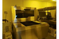
400nm To 410nm Laser Direct Imaging 133LPI Decal Heat Transfer
|
|
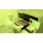
3D Glass Cover Panel LDI Laser Direct Image Exposure Machine For Vehicle Glass
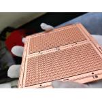
In the world of PCB Manufacturing, it is important to stay as up-to-date as possible with industry trends. This is because, circuit boards are constantly evolving and getting more complex, due to miniaturization trends in the electronics industry. These changes have caused the traditional imaging process for HDI PCBs to provide inadequate results. In response to new electronics tendencies, the PCB manufacturing industry has come up with a new imaging technique known as Laser Direct Imaging. Below you will find an introductory guide to this process.
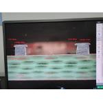
Advanced Automation Line for 3D Cover Glass This automation line is used to produce BM patterning process on 3D glass for smart phone; 3D raw glass material input by fully equipped automatic loading machine, followed by plasma cleaner, automatic spraying machine, tunnel oven, DLP exposure machine, developing and washing machine, final goods output by unloading machine; Up to 30um resolution, over 95% of yield, thinning BM layer that easier for assembly, higher pattern quality and lower cost of ownership for customers;
*Specifications subject to change without notice
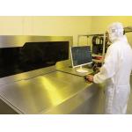
About US GIS Intelligent Inc., subsidiary corporation of GIS Tech Inc., focusing on advanced solution for Lithium battery fabrication and 3D cover glass patterning. GIS Tech Inc. was established by founders from U.S in 2015, Suzhou China, developing Digital Lighting Processing (DLP) specially for different industry patterning solution needs, which enable MEMS/Glass /PCB/Screen printing manufacturers to achieve the best imaging results with the highest throughput. We are the leader in automation solution for 3D cover glass in the world, which was used to produce high quality BM patterning on large curvature glass by DLP photolitho. Our DLP systems powered by Dr. Takeda, together with GIS’s semiconductor laser diodes technologies to achieve enhanced Depth-of-Focus for 3D topography changes, as well as patterning uniformity. The core team of GIS Tech come from the top 500 international companies from the United States. Based on over 20 years experience of semiconductor technology, automation and materials teams, we fully understand and master the industry‘s development trend and cutting-edge technology. Our expertise in transferring patterns on cover glass materials at high curvature level and irregular shaped enables customers to transform possibilities into reality, especially for 3C smart electronics and automobile cover glass.
|
||||||||||||||||||||||||||||
| Product Tags: 410nm laser direct imaging 400nm laser direct imaging 133LPI direct imaging pcb |

|
High Precision Laser Print Equipment Support The Board To Set Text |
|
High Precision Laser Direct Printing Machine With 405 Nm/25-50 W For Serial Number |

|
610mm*710mm Laser Imaging Equipment With 25/25μM Line Width / Spacing |
|
0.05-7mm Board Laser Direct Imaging Machine With Fixed / Auto / Interval / Partition Scale |
|
Ceramic Substrate Laser Imaging Equipment ±10μm Outer Alignment Accuracy |
|
Gerber 274x Laser Direct Imaging Machine 20μM Inner Alignment Accuracy |