
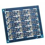
20 Layer Special Pcb Backdrilling Process On Pad Communication Multilayer
|
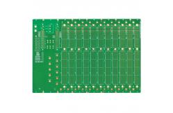
Backdrilling+Hole On Pad Communication Multilayer PCBThe Backdrilling+Hole On Pad Communication Multilayer PCB is the special process PCB circuit board developed and produced by Shenzhen Quanhong Electronics Co., Ltd. the HDI board is made of FR-4 material, surface gold deposition and laser drilling. The minimum line width and line spacing can reach 75um and the minimum hole diameter can reach 0.1mm. The buried blind hole circuit board is widely used in digital cameras, notebooks, mobile phones and other electronic products and automotive electronics. Rigid PCB Manufacturing Capability
FAQ: Q: What service do you have?
Q: What is needed for PCB & PCBA quotation?
Q: How to keep our product information and design file secret ?
Q: What are the main products of your PCB/PCBA services?
Q: What is your minimum order quantity (MOQ)?
Q: Are you factory? FASTPCB:Shangxing West Industrial Zone, Xihuan Road, Shajing Street, Bao 'an District, Shenzhen, Guangdong province, China
|
|||||||||||||||||||||||||||||||||||||||||||||||||||||||||||||||||||||||||||||||||||
| Product Tags: 20 Layer Special Pcb Backdrilling Backdrilling Pcb 20 layer pcb | |||||||||||||||||||||||||||||||||||||||||||||||||||||||||||||||||||||||||||||||||||
|
Tg170 Tg180 Fr4 Copper Clad Special PCB ENIG OSP Selective Surface |
|
4 Layer Special PCB 1.6 Mm 94v0 Fr-4 Pcb Board Half Hole Module |

|
6 Layer Special PCB Printed Circuit Board Fr-4 Optical Fiber Module |
|
High Density Pcb Multi Layer Printed Circuit Board 2.0mm |
|
HLC High Layer Count Pcb For 5G Era |
|
FR-4 Sy S1000-2 8 Layers Special PCB Motherboard Industrial Control 1.6mm |