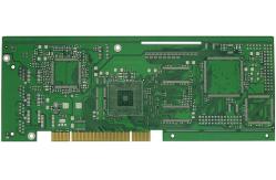
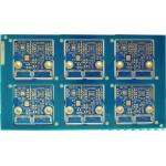
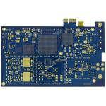
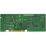
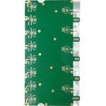
FPGA High Speed Printed Circuit BoardThe FPGA High Speed Printed Circuit Board is a high-speed circuit
board developed and produced by Shenzhen Quanhong Electronics Co.,
Ltd. It is made by pure pressing of shengyi S1000-2M
high-speed materials, surface gold deposition and other production
processes. It is widely used in the field of high-speed computers
and high-end servers in cloud data centers. The products have the
characteristics of stability and durability. | Item | HDI Advanced Technology | | 2019 | 2020 | 2021 | | Structure | 5+n+5 | 6+n+6 | 7+n+7 | | HDI Stack Via | AnyLayer(12L) | AnyLayer(14L) | AnyLayer(16L) | | Board Thickness(mm) | Min. 8L | 0.45 | 0.4 | 0.35 | | Min. 10L | 0.55 | 0.45 | 0.4 | | Min. 12L | 0.65 | 0.6 | 0.55 | | MAX. | | 2.4 | | | Min. Core Thickness ( um ) | 50 | 40 | 40 | | Min. PP Thickness ( um ) | 30(#1027PP) | 25(#1017PP) | 20(#1010PP) | | Base Copper Thickness | Inner Layer ( OZ) | 1/3 ~ 2 | 1/3 ~ 2 | 1/3 ~ 2 | | Outer Layer ( OZ ) | 1/3 ~ 1 | 1/3 ~ 1 | 1/3 ~ 1 | | Item | HDI Advanced Technology | | 2019 | 2020 | 2021 | | Min. Mechanical Drill hole size(um) ** | 200 | 200 | 150 | | Max. Through Hole Aspect Ratio * | 8:1 | 10:1 | 10:1 | | Min. Laser via/Pad Size ( um ) | 75/200 | 70/170 | 60/150 | | Max. Laser Via Aspect Ratio | 0.8:1 | 0.8:1 | 0.8:1 | | Laser Via on PTH(VOP)design | Yes | Yes | Yes | | Laser X type through hole(DT≤200um) | NA | 60~100um | 60~100um | | Min. LW/S (L/S/Cu, um) | Inner Layer | 45 /45 /15 | 40/ 40/ 15 | 30/ 30 /15 | | outer Layer | 50 /50/ 20 | 40 /50 /20 | 40 /40 /17 | | Min BGA Pitch (mm) | | 0.35 | 0.3 | 0.3 | | Item | HDI Advanced Technology | | 2019 | 2020 | 2021 | | Solder mask Registration (um) | +/- 30 | +/- 25 | +/- 20 | | Min. Solder Mask Dam (mm) | 0.07 | 0.06 | 0.05 | | PCB Warpage Control | >= 50ohm | +/-10% | +/-8% | +/- 5% | | < 50ohm | +/- 5ohm | +/- 3ohm | +/- 3ohm | | PCB Warpage Control | ≤0.5% | ≤0.5% | ≤0.5% | | cavity Depth accuracy (um) | Mechanical | +/- 75 | +/- 75 | +/- 50 | | Laser directly | +/- 50 | +/- 50 | +/- 50 | | Surface Finishing | OSP,ENIG,Immersion Tin,Hard Au, Immersion Ag | OSP,ENIG,Immersion Tin,Hard Au,Immersion Ag, ENEPIG |
| Item | HLC Advanced Technology | | 2019 | 2020 | 2021 | | Max Panel Width (inch) | 25 | 25 | 25 | | Max Panel Length (inch) | 29 | 29 | 29 | | Max Layer Count (L) | 16 | 18 | 36 | | Max Board thickness (mm) | 3.2 | 4 | 6 | | Max Board thickness Tolerance | +/-10% | +/-10% | +/-10% | | Base copper Thickness | Inner layer ( OZ ) | 4 | 6 | 8 | | Outer Layer ( OZ ) | 2 | 3 | 4 | | Min DHS ( mm ) | 0.2 | 0.15 | 0.15 | | PTH Size Tolerance ( mil ) | +/-2 | +/-2 | +/-2 | | Back Drill (stub)( mil ) | ~ 3 | ~ 2.4 | ~ 2 | | Max. AR | 12:1 | 16:1 | 20:1 | | Item | HLC Advanced Technology | | 2019 | 2020 | 2021 | | M-drill tolerance | Inner layer ( mil ) | DHS + 10 | DHS + 10 | DHS + 8 | | Outer Layer ( mil ) | DHS + 8 | DHS + 8 | DHS + 6 | | Solder mask Registration (um) | +/- 40 | +/- 30 | +/- 25 | | Impedance control | ≥50ohms | +/-10% | +/-10% | -/-8% | | <50ohms | 5 Ω | 5 Ω | 4 Ω | | Min LW/S (Inner)@1oz base Cu ( mil ) | 3.0 / 3.0 | 2.6 / 2.6 | 2.5 / 2.5 | | Min LW/S (Outer)@1oz Cu ( mil ) | 3.5 / 3.5 | 3.0 / 3.5 | 3.0 / 3.0 | | Max dimple for POFV ( um ) | 30 | 20 | 15 | | Surface Finishing | ENIG, Immersion Ag, OSP, HASL, Immersion Tin, Hard Au |
| Item | SMT Capability | | 2019 | 2020 | 2021 | | Min board thickness ( mm ) | 0.1 | 0.06 | 0.05 | | Max. board size ( mm ) | 200 x 250 | 250 x 300 | 250 x 350 | | Chip component ( L, C, R etc. ) | Minimum size | 1005 | 1005 | 1005 | | Connector | 0.5 mm pitch | Y | Y | Y | | 0.4 mm pitch | Y | Y | Y | | 0.35 mm pitch | Y | Y | Y | | High density component : | 0.5 mm pitch | Y | Y | Y | | TSOP, QFP, QFN, LGA, BGA etc. | 0.4 mm pitch | Y | Y | Y | | | 0.35 mm pitch | Y | Y | Y | | Reflow | N2 reflow | No | Y | Y | | Under-fill | Fill under chip | Manual | Auto | Auto | | ACF attach | Gold finger pitch | N/A | 0.3 mm | 0.2 mm | | Inspection | Component position, direction, missing etc. | Manual check with 10 x scope | Auto AOI inspection | Auto AOI inspection | | Solder paste thickness | Measure once per shift | 1 line auto full area, online SPI | All lines auto full area, online SPI |
Packaging & Delivery | Packaging Details: | Inner: vacuum packing or Anti-static package,
Outer: export carton
or according to the customer's requirement. | Port: | Shenzhen or Hongkong | Lead Time: | Quantity(Pieces) | 1-10 | 11-100 | 101-1000 | >1000 | | Est. Time(days) | 3-5 | 3-5 | 7-9 | To be negotiated |
FAQ:
Q: What service do you have?
FASTPCB: We provide turnkey solution including PCB fabrication,
SMT, plastic injection & metal,final assembly, testing and
other value-added service.
Q: What is needed for PCB & PCBA quotation?
FASTPCB: For PCB: Quantity, Gerber file and technic
requirements(material,size, surface finish treatment, copper
thickness,board thickness).
For PCB: PCB information, BOM,Testing documents.
Q: How to keep our product information and design file secret ?
FASTPCB: We are willing to sign a NDA effect by customers side
local law and promising tokeep customers data in high confidential
level.
Q: What are the main products of your PCB/PCBA services?
FASTPCB: Automotive, Medical, Industry Control, IOT, Smart Home,
Military, Aerospace.
Q: What is your minimum order quantity (MOQ)?
FASTPCB: Our MOQ is 1 PCS, sample and mass production all can
support.
Q: Are you factory?
FASTPCB:Shangxing West Industrial Zone, Xihuan Road, Shajing
Street, Bao 'an District, Shenzhen, Guangdong province, China
|