
141 - 150 of 258
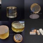
polish srtio3 crystal wafer
Selling leads
|
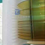
4 inch Diameter LiNbO3 Wafer 0.25mol% Er dope or 5mol% MgO dope for Optical Applications LiNbO3 (LN) crystal has stable physical, chemical and ...
2025-08-02 00:14:07
|

|
...photonic applications. Renowned for their exceptional electrical insulation, high thermal conductivity, and chemical stability, MgO Wafers are the ...
2024-12-10 00:36:40
|
|
... in the VIS and UV is approx. The transmission range of significantly cheaper JGS2 wafers is shifted towards longer wavelengths when compared with ...
2024-12-09 20:34:25
|
|
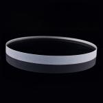
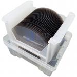
X-cut Y-cut Crystal Quartz Ring IEEE standard Double Side Lapped for Pressure Sensor There are a variety of piezoelectric materials that can conduct ...
2025-08-02 00:14:07
|
|
...Crystal Quartz Wafer for High-Performance Pressure Sensing Solutions Single Crystal Quartz Rings Elevate your scientific, industrial, or optical ...
2025-08-02 00:14:07
|
|
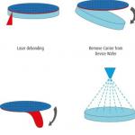
Carrier wafer made of Glass and Monocrystal Quartz for Thin Wafer Handling System Based on the market demand for small devices, there is ongoing wafer ...
2024-12-09 20:34:25
|
|
..., and a wide transparency range going from ultraviolet to infrared. It is desirable that LiTaO3 wafer was a smooth surface in order to function ...
2025-08-02 00:14:07
|
|
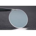
...Wafer Sapphire Wafer 330um 430um Thick Our sapphire wafers are the epitome of precision and quality, crafted from the purest sapphire crystal. ...
2024-12-09 20:34:25
|
|
...piezoelectric materials. Developed by our team of experts, these wafers are made from Langasite Crystal and have superior performance compared to ...
2024-12-09 23:27:58
|
|
... acoustic attenuation. Typical cut angle for SAW application is 36°Y, 42°Y, X-cut etc. The Lithium Tantalate reduction technology makes the wafer ...
2024-12-09 20:34:25
|