
271 - 280 of 365
optical windows crystal wafer
Selling leads
|
...Wafer 4'' 6'' 8'' for MEMS Devices Glass wafers made of borosilicate glass are often used in Semiconductor and MEMS industry in a wide variety of ...
2024-12-09 20:34:25
|
|
...Wafers Thickness 0.35±0.025mm in Fused Silica Borosilicate BonTek is a recognized participant in the manufacture of transparent Glass wafers. Many ...
2024-12-09 20:34:25
|
|
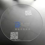
Crystal Lithium Tantalate Wafer 3inch 4inch with Customized Orientation and Thickness The present neutron study, based on 77 independent F meas, has ...
2024-12-09 20:34:25
|
|
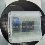
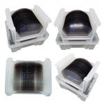
AT ST Cut Quartz Crystal Round Blanks and Wafer Piezoelectric materials exhibit a directionally related electric charge when subjected to pressure and ...
2025-07-29 00:13:51
|
|
... and H2. Bulk conductivity and optical transmittance of the black LiNbO3 and black LiTaO3 wafers were measured. The results showed that the ...
2024-12-09 20:34:25
|
|
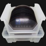
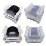
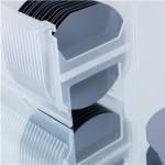
...Wafer for Higher Frequency SAW devices Free-pyro black LiNbO3 and LiTaO3 wafers were prepared successfully by chemical reduction under a mixed ...
2024-12-09 20:34:25
|
|
...Wafer for Surface Acoustic Wave IDT Applications Free-pyro black LiNbO3 and LiTaO3 wafers were prepared successfully by chemical reduction under a ...
2024-12-09 20:34:25
|
|
...Wafer for High-Power-Frequency Converters Push the boundaries of technology with our cutting-edge LiTaO3 Wafers. As a premier material for high...
2024-12-10 00:26:38
|

|
...Wafers The Optimal Material for High-Performance Optoelectronics Doped LN Wafers: MgO:LN the 5mol% MgO-doped LiNbO3 Wafers, the perfect blend of ...
2024-12-10 00:36:40
|

|
...-edge material known for its exceptional piezoelectric, ferroelectric, and optical properties. Ideal for a wide range of advanced applications, SLT ...
2025-03-06 16:31:05
|