
81 - 90 of 176
optical sapphire crystal substrate
Selling leads
|
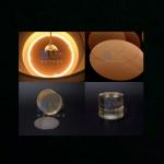
...density is 4.64 g/cm3, Mohs hardness is 5, refractive index no=2.286 ne=2.203 at 632.8nm. It is ferroelectric crystal, Curie point 1150°C. With ...
2025-07-17 00:19:03
|
|
...density is 4.64 g/cm3, Mohs hardness is 5, refractive index no=2.286 ne=2.203 at 632.8nm. It is ferroelectric crystal, Curie point 1150°C. With ...
2025-07-17 00:19:03
|
|
... over a wide range from the UV through to the IR and widely used to fabricate optical components. BaF2 barium fluoride scintillation crystals are ...
2024-12-09 20:34:25
|
|
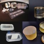
...Sapphire Wafer Used As Infrared Windows Night Infrared Scope Night Vision Camera Sapphire wafers are the epitome of modern semiconductor technology...
2024-12-09 20:34:25
|
|
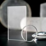
...Sapphire Wafers The Ultimate Solution for High-Performance Applications Unlock unparalleled precision and durability with our premium Sapphire ...
2025-04-21 22:24:41
|
|
...Crystal Quartz Wafer for SAW Components Unleash the Power of Monocrystalline Quartz Wafers for Your Cutting-Edge Applications! Discover the ...
2025-07-17 00:19:03
|
|
... range from the UV through to the IR and widely used to fabricate optical components. BaF2 barium fluoride scintillation crystals are characterized ...
2024-12-09 20:34:25
|
|
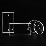
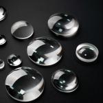
...Optics Used For Special Optical Windows The calcium fluoride(CaF2) crystal has a high transmittance in the range of 0.13~11.3 um, can reach 95%, ...
2024-12-09 20:34:25
|
|
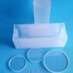
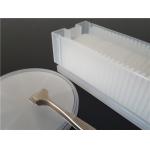
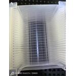
X-cut Z-cut Single Crystal Quartz Wafer double side polish for Optical application You can buy Quartz wafer for SAW components from BonTek. We are a ...
2024-12-09 20:34:25
|
|
...Crystal Wafer for Semiconductor and MEMS Applications The piezoelectric effect in a crystal is explained as that there will be the development of ...
2025-07-17 00:19:03
|