31 - 40 of 98
8 inch piezo wafer
Selling leads|
... response in electrical simulation is called the opposite of the piezoelectric effect. In crystalline materials, the number of electrical dipoles ...
2024-12-09 20:34:25
|
|
...Wafers widely used in Telecommunications Lithium Tantalate (LT, LiTaO3) has unique properties, which as a material finds uses in Electro-Optical ...
2025-07-30 00:13:57
|
|
Single Crystal Quartz Cut Into Wafer With Different Orientation Piezo quartz is the highly symmetric shape of the single crystal, is characterized by ...
2024-12-09 21:03:49
|
|
...widely used applications are surface acoustic wave devices, bulk acoustic wave devices, piezo-electric transducers, pyroelectric infrared sensor ...
2025-07-30 00:13:57
|
|
...precision and durability, our single-crystal quartz wafers are the ideal solution. These wafers, crafted from pure quartz, exhibit exceptional ...
2025-07-30 00:13:57
|
|
... Quartz Wafers for High Temperature Applications Customized Orientation Options with 3 Inch and 4 Inch Sizes our Single Crystal Quartz Wafers, the ...
2025-07-30 00:13:57
|
|
...inch 100mm SiO2 Fused Silica Wafers Corning 7980 in stock for Immediate Shipment High quality 4 inch SiO2 Fused Silica wafers are in stock for ...
2024-12-09 20:34:25
|
|
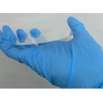
... ultra-thin LiTaO3 wafers, boasting a wafer-level thickness of 20um and a diameter extending up to 4 inches, are the epitome of this refined ...
2024-12-09 22:59:53
|
|
...Inch Lithium Niobate Wafer With Surface Roughness Ra 0.5nm LiNbO3 Introduction LiNbO3 wafers, also known as lithium niobate wafers, are essential ...
2024-12-09 22:36:19
|
|
...an ideal material for Anodic bonding. BonTek provides borosilicate wafers from 2 to 14 inches diameter, the thickness is 100um up with low ...
2024-12-09 20:34:25
|

