
21 - 29 of 29
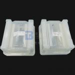
200mm mems wafer
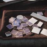
Selling leads
|
3 Inch 4 Inch Single Crystal Quartz Wafer AT-Cut ST-Cut for SAW and MEMS BonTek Optoelectronics provides high quality Single Crystal Quartz wafers in ...
2025-07-25 00:18:38
|
|
Product Description: Fused Silica Wafer is a high-performance, cost-effective IC Silicon Wafer product that is widely used in the semiconductor, MEMS ...
2024-12-09 22:58:07
|
|
...200mm Fused Silica Wafer Borosilicate Customized Thickness with Flat or Notch Edge ground BonTek works a lot with fused silica, fused quartz, ...
2024-12-09 20:34:25
|
|
6 inch 0.5mm Borofloat 33 Glass Substrate for Semiconductor Industry and MEMS With its unique physical and chemical properties, BOROFLOAT33 has become ...
2024-12-09 20:34:25
|
|
... range (>85% @185nm, >90% from 200nmto 2000nm). The most seen brand/grade is JGS1, Corning 7980 and SK1300. BonTek supply these wafers with ...
2025-07-25 00:18:38
|
|
...Wafer JGS3 C7979 and SK1310 with Very Low OH content There are also IR grade Fused Silica wafers with transmission from 185nm to 350nm. The IR ...
2024-12-09 20:34:25
|
|
Revolutionizing Chip Fabrication Precision Innovation and Excellence At the forefront of advanced chip foundry services, we empower innovation by ...
2025-04-21 22:24:41
|
|
Borofloat 33 Glass Substrate for High-Temperature Applications and Precision Operations The Epitome of Precision & Durability in Glass Solutions ...
2024-12-10 00:16:16
|
|
...versatility for advanced electronic and optical applications. Renowned for their exceptional dielectric properties, high permittivity, and tunable ...
2025-03-06 16:31:04
|