
11 - 20 of 44
0 5mm silicon wafer
Selling leads
|
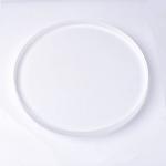
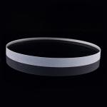
...Wafer and BF33 C7980 BK7 H-K9L Glass Wafers The glass wafers are widely used as bonding material with silicon wafers in semiconductor industry. ...
2024-12-09 20:34:25
|
|
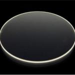
.... Fused Silica Wafer has very low thermal expansion coefficient, excellent electrical insulation properties, and superior thermal shock resistance. ...
2024-12-09 22:58:07
|
|
... wafers this is the Kyropoulos method (abbreviated to Ky or Kr). The Kyropoulos method is a continuation of the Czochralski method (CZ) which is ...
2024-12-09 20:34:25
|
|
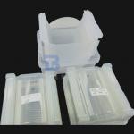
Y128-Cut 4 inch 0.5mm LiNbO3 Wafer DSP pack in Cassette Lithium Niobate (LiNbO3, LNO), an uniaxial ferroelectric with a very high Curie temperature ...
2025-08-01 00:14:26
|

|
...5mm 8 Inch Lithium Niobate Wafer With Surface Roughness Ra 0.5nm LiNbO3 Introduction LiNbO3 wafers, also known as lithium niobate wafers, are ...
2024-12-09 22:36:19
|
|
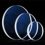
... in the VIS and UV is approx. The transmission range of significantly cheaper JGS2 wafers is shifted towards longer wavelengths when compared with ...
2024-12-09 20:34:25
|
|
...TTV of ≤3μm, thickness of 0.5mm-3mm and roundness of edge grinding. With its high-end material and strict quality control, Sapphire Wafer provides ...
2024-12-09 23:10:26
|
|
Product Description: Fused Silica Wafer is a high-performance, cost-effective IC Silicon Wafer product that is widely used in the semiconductor, MEMS ...
2024-12-09 22:58:07
|
|
...an ideal material for Anodic bonding. BonTek provides borosilicate wafers from 2 to 14 inches diameter, the thickness is 100um up with low ...
2024-12-09 20:34:25
|
|
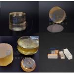
...5mm 128Y-cut Black Lithium Niobate Wafer SAW Application IDT use Ra Roughness 1nm The reduction technology is used to produce Black Lithium Niobate ...
2024-12-09 20:34:25
|