
311 - 320 of 540 Selling leads
|
Stepanov s Method Grown Sapphire Wafer 4inch C-plane for Optical Applications Our exquisitely crafted Sapphire Wafers – a gemstone-like innovation for ...
2026-03-27 20:05:03
|

|
Product Description: This Quartz Wafer is available in various sizes, with Primary Flat dimensions of 22mm, 32.5mm, 42.5mm, 57.5mm/notch, notch, notch...
2026-03-27 20:05:03
|

|
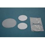
Product Description: The Fused Silica Wafer has a low total thickness variation (LTV) of less than 2µm, which makes it ideal for applications that ...
2026-03-27 20:05:03
|

|
Product Description: One of the key features of this product is its polished side Ra, which is less than 1.0nm or specific per requested, making it ...
2026-03-27 20:05:03
|

|
Product Description: The Fused Silica Wafer is available in different sizes, thicknesses, and surface finishes. The polished side Ra is less than 1...
2026-03-27 20:05:03
|

|
Product Description: Our Fused Quartz Wafer is designed with precision and accuracy to meet the standards required by the semiconductor industry. It ...
2026-03-27 20:05:03
|

|
Product Description: Features: Product Name: JGS1 JGS2 JGS3 Glass and Quartz wafer for Superior Optical Clarity Chemical Stability Material: UV Fused ...
2026-03-27 20:05:03
|
|
2" 3" 4" 6"Sapphire Wafer Al2O3 Crystal Substrate Double Side Polished For Optical In today's rapidly evolving world of electronic...
2026-03-27 20:05:03
|

|
Borofloat 33 Glass Substrate for Semiconductor Industry and MEMS BOROFLOAT33 Glass for Various Application Unlock the potential of your applications ...
2026-03-27 20:05:03
|

|
4'' 6" Piezoelectric Crystal Lithium niobate LN LiNbO3 Wafer for Optical Applications Elevate your technology with our premium Lithium Niobate ...
2026-03-27 20:05:03
|