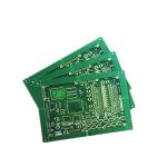
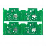
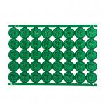
Multilayer Board PCB Manufacturing Motherboard Printed Circuit
Board PCB Manufacturing Introduce:
PCB and PCBA, as important components in the electronics industry,
play a key role in electrical interconnection and circuit support.
It is widely used in industrial control, communication modules,
medical, automotive electronics, security equipment, and other
industries. PCB printed circuit board provides the fixing and
electrical connection of electronic components, while PCBA, as the
processing process of the printed circuit board, completes the
assembly and welding of components. PCB Manufacturing Parameters: | Item | Technical Parameter | | Layer | 2-64 | | Thickness | 0.3-6.5mm | | Copper Thickness | 0.3-12 oz | | Min Mechanical Hole | 0.1mm | | Min Laser Hole | 0.075mm | | HDI | 1+n+1,2+n+2,3+n+3 | | Max Aspect Ratio | 20:01 | | Max Board Size | 650mm*1130mm | | Min Width/Space | 2.4/2.4mil | | Min Outline Tolerance | ±0.1mm | | Impedance Tolerance | ±5% | | Min PP Thickness | 0.06mm | | Bow &Twist | ≤0.5% | | Materials | FR4, High-Tg FR4, Rogers, Nelco, RCC, PTFE, M4, M6, TU862, TU872 | | Surface Finished | HASL, HASL Pb Free Immersion Gold/Tin/Silver Osp, Immersion
Gold+OSP | | Special Capability | Gold Finger Plating, Peelable, Carbon ink |
PCB Manufacturing Features:
1. One-line service from prototype to production
2. Multi-layer production: 2-68 layers
3. TPS lean production, high reliability, IATF16949, UL
certification
4. SMT capacity: 14 million advertising spaces per day |