
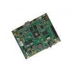
Embedded Resistor PCB Layout Design Gold Finger Plating Pcb Design Services
|
|
Embedded Resistor PCB Layout Design Gold Finger Plating Testability
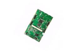
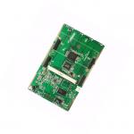
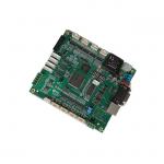
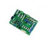
PCB Layout Design Description: The PCB boards we produce include POP boards, ordinary boards, FPC boards, rigid-flex bonding boards, metal baseplates, etc. They are widely used in industrial control, medical care, automotive electronics, communications, and the Internet. The product is RoHS-compliant lead-free assembly/non-RoHS assembly. SMT, post welding, assembly to testing one-stop service supports flexible supply.
FAQ: Q: What are the benefits of choosing us?
Q: What are the payment terms we can accept?
In high-speed design, the characteristic impedance of controlled impedance boards and lines is one of the most important and common problems. First understand the definition of a transmission line: A transmission line consists of two conductors of a certain length, one for sending a signal and the other for receiving a signal (remember the concept of "loop" instead of "ground"). In a multilayer board, each trace is part of a transmission line, and the adjacent reference plane can act as a second trace or return. The key to a line being a "good" transmission line is to keep its characteristic impedance constant throughout the line. |
||||||||||||||||
| Product Tags: Nelco PCB Layout Design Embedded Resistor PCB Layout Design Gold Finger Plating Pcb Design Services |
|
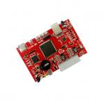
Embedded Resistor PCB Layout Design Gold Finger Plating Pcb Design Services |
|
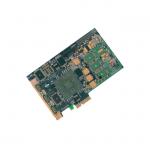
Metal Substrate High Speed Pcb Design PTFE Producibility Board Layout Design |
|
Embedded Capacitor PCB Layout Design High Tg FR4 Maintainability |
|
12 SMT PCB Circuit Layout Flexible Carbon Ink Pcb Layout Services |
|
Step Groove Layout Pcb Design Designability Rogers Multilayer Circuit Board |
|
High Frequency PCB Layout Design TU862 Printed Circuit Board Design Industrial |