
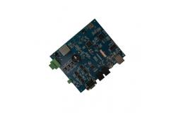
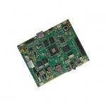
Blind Hole Boards Print Layout PCB Design And Layout Services Rogers
|
|
Blind - Hole Boards PCB Layout Design Back Drill Gold Finger Plating Rogers
PCB Layout Design Description: The PCB assembly we produce includes rapid turn prototype PCB assembly, SMT/SMD assembly, through-hole assembly, hybrid technology (SMT/through-hole), turnkey assembly, consignment assembly, etc. They are widely used in industrial control, medical care, automotive electronics, communications, and the Internet. SMT, post welding, assembly to testing one-stop service supports flexible supply.
The printed circuit board has good product consistency, and it can adopt a standardized design, which is conducive to the realization of mechanization and automation in the production process. At the same time, the entire printed circuit board that has been assembled and debugged can be used as an independent spare part, which is convenient for the exchange and maintenance of the whole product. At present, printed circuit boards have been widely used in the manufacture of electronic products. |
||||||||||||||||||||||||||||||||||
| Product Tags: Blind Hole Boards Print Layout PCB Print Layout PCB Rogers Rogers pcb design and layout services |
|
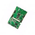
Embedded Resistor PCB Layout Design Gold Finger Plating Pcb Design Services |
|
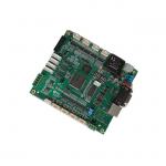
Metal Substrate High Speed Pcb Design PTFE Producibility Board Layout Design |
|
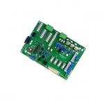
Embedded Capacitor PCB Layout Design High Tg FR4 Maintainability |
|
12 SMT PCB Circuit Layout Flexible Carbon Ink Pcb Layout Services |
|
Step Groove Layout Pcb Design Designability Rogers Multilayer Circuit Board |
|
High Frequency PCB Layout Design TU862 Printed Circuit Board Design Industrial |