
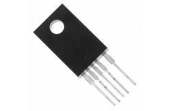
FSCQ0765RT Switching Power Mosfet Green Mode Fairchild Power Switch ( FPS )
|
|
FSCQ-Series FSCQ0565RT / FSCQ0765RT / FSCQ0965RT / FSCQ1265RT FSCQ1465RT / FSCQ1565RT / FSCQ1565RP Green Mode Fairchild Power Switch (FPSTM)
Features • Optimized for Quasi-Resonant Converter (QRC) • Advanced Burst-Mode Operation for under 1W Standby Power Consumption • Pulse-by-Pulse Current Limit • Over Load Protection (OLP) - Auto Restart • Over Voltage Protection (OVP) - Auto Restart • Abnormal Over Current Protection (AOCP) - Latch
• Internal Thermal Shutdown (TSD) - Latch • Under Voltage Lock Out (UVLO) with Hysteresis • Low Startup Current (typical : 25uA) • Internal High Voltage SenseFET • Built-in Soft Start (20ms) • Extended Quasi-Resonant Switching
Applications • CTV • Audio Amplifier
Related Application Notes • AN4146 - Design Guidelines for Quasi-Resonant Converters Using FSCQ-Series Fairchild Power Switch. • AN4140 - Transformer Design Consideration for Off-Line Flyback Converters Using Fairchild Power Switch.
Description In general, a Quasi-Resonant Converter (QRC) shows lower EMI and higher power conversion efficiency compared to conventional hard-switched converter with a fixed switching frequency. Therefore, a QRC is well suited for noisesensitive applications, such as color TV and audio. Each product in the FSCQ-Series contains an integrated Pulse Width Modulation (PWM) controller and a SenseFET, and is specifically designed for quasi-resonant off-line Switch Mode Power Supplies (SMPS) with minimal external components.
The PWM controller includes an integrated fixed frequency oscillator, under voltage lockout, leading edge blanking (LEB), optimized gate driver, internal soft start, temperature-compensated precise current sources for a loop compensation, and self protection circuitry. Compared with a discrete MOSFET and PWM controller solution, the FSCQSeries can reduce total cost, component count, size, and weight, while simultaneously increasing efficiency, productivity, and system reliability. These devices provide a basic platform that is well suited for cost-effective designs of quasi-resonant switching flyback converters.
MAXIMUM OUTPUT POWER TABLE(3)
Notes: 1. Maximum practical continuous power in an open frame design at 50°C ambient. 2. 230 VAC or 100/115 VAC with doubler. 3. The junction temperature can limit the maximum output power.
Typical Circuit
Internal Block Diagram
Pin Configuration
Stock Offer (Hot Sell)
|
|||||||||||||||||||||||||||||||||||||||||||||||||||||||||||||||||||||||||||||||||||||||||||||||||||||||||||||||||||||||||||||||||||||||||||||||||||||||||||||||||||||||||||||||||||||
| Product Tags: power mosfet ic silicon power transistors |
|
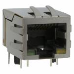
Original Connect RJ45 Ethernet Jack Plug J00-0065NL for PBC Board |
|
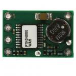
PTH04000WAH NEW AND ORIGINAL STOCK |
|
UPS161 Synchronizing signal controlling CMOS LSI tv circuit boards led driver circuit board |
|
BSM100GB60DLCHOSA1 NEW AND ORIGINAL STOCK |
|
FF150R12RT4HOSA1 NEW AND ORIGINAL STOCK |
|
FF100R12RT4HOSA1 NEW AND ORIGINAL STOCK |