
141 - 150 of 449
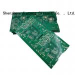
osp 1 layer pcb
Selling leads
|
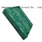
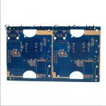
... PCBs. It provides multiple options for material, thickness, line width, impedance control, silkscreen color and other necessary parameters. Our ...
2025-07-12 00:27:43
|
|
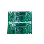
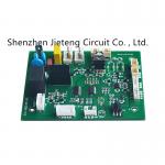
...Layer PCB Fabrication is a comprehensive process for creating multi-level printed wiring boards. It involves the manufacture and assembly of ...
2025-07-12 00:27:43
|
|
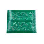
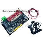
...layer PCB is designed using the latest technology and advanced manufacturing techniques, with a thickness of 2.0mm, 2OZ copper thickness, the black ...
2025-07-12 00:27:43
|
|
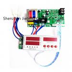
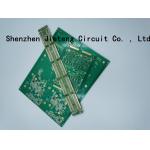
pcb control board Automobile panel industrial control panel medical instrument main control panel Essential details Place of Origin: Guangdong, China ...
2025-07-12 00:27:43
|
|
... Min. Line Spacing: 6mil Surface Finishing: HASL,Immersion gold,Flash gold, plated silver, OSP Application: Electronic Products Solder Mask: Green ...
2025-07-12 00:27:43
|
|
...PCB Board Board Control Board PCBA electronic product program development Essential details Model Number: 20220226 Place of Origin: Guangdong, ...
2024-12-09 17:47:37
|
|
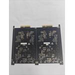
...PCB & PCB Assembly Place of Origin: Guangdong, China Base Material: FR-4/CEM-1/CEM-3/Polyimild/PTFE/Rogers Copper Thickness: 0.4-2mil(10-50um) ...
2025-07-12 00:27:43
|
|
... Min. Hole Size: 0.1MM Min. Line Width: 0.04MM Min. Line Spacing: 0.04MM Surface Finishing: HASL / OSP / ENIG /
2025-07-12 00:27:43
|
|
.... Hole Size: 0.2mm Min. Line Width: 3mil Min. Line Spacing: 3mil Surface Finishing: HASL-LF/OSP/ENIG etc Board Size:
2024-12-09 17:47:37
|
|
...PCB assembly/PCB manufacturer in China Essential details Place of Origin: Guangdong, China Base Material: Shengyi material or Lianmao material ...
2025-07-12 00:27:43
|