
21 - 30 of 178
pcb aoi wafer inspection
Selling leads
|
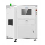
... product. The machine is also designed with manual width adjustment, giving operators the ability to adjust the system to meet their specific needs...
2026-06-01 00:25:56
|
|
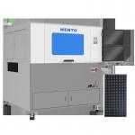
...Defective die removing, residues cleaning, solder paste/adhesive printing, die bonding, solder curing, luminescence inspection Wafer size 3x5mil...
2026-06-01 00:25:56
|

|
... optical system (light source consistency) 5. High stability integrated casting platform Application scope: solder joint and mounted device ...
2026-06-01 00:25:56
|

|
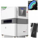
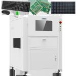
Product Description: The easy-to-use Drag and Drop programming interface of the Automated Optical Inspection Machine allows for effortless and ...
2026-06-01 00:25:56
|
|
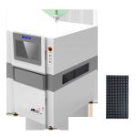
Model M20 Series Mini LED appearance inspection M2012 Inspection Inspection items Missed bonding, wrong bonding, die damaged, die offset, die tilted, ...
2026-06-01 00:25:56
|

|
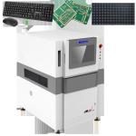
...PCBs. This camera type is especially useful in detecting defects that are difficult to spot with the naked eye. It enables the machine to identify ...
2026-06-01 00:25:56
|
|
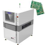
K20 series 2D Automated Optical InspectionOnline dual track 2D Automated Optical Inspection Online dual track Model K2012DT Testing Capability Test ...
2026-06-01 00:25:56
|
|
...AOI features 1. High cost performance 2. Standard 5 million global exposure industrial color camera 3. The first company in China to use large...
2026-06-01 00:25:56
|
|
Product Description: Device model K2012DW Detection capacity Detection items CHIP component body, CHIP component solder joints, characters, DIP solder ...
2026-06-01 00:25:56
|
|
Product Description: 3D Solder Paste Inspection Device model K3205 Detection capacity Detection items Miss print, over solder, insufficient solder, ...
2026-06-01 00:25:56
|