
101 - 110 of 188
pcb aoi wafer inspection
Selling leads
|
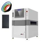
...inspection area is also impressive, with up to 610mm x 460mm of coverage. Investing in an automated optical inspection machine is a smart decision ...
2026-10-23 00:42:53
|
|
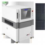
M20EL Series Mini LED luminescence inspection Model M2012EL Inspection Inspection items Bad die, over luminescence, under luminescence, chroma anomaly ...
2026-10-23 00:42:53
|
|
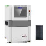
Model M20 Series Mini LED appearance inspection M2065 Inspection Inspection items Missed bonding, wrong bonding, die damaged, die offset, die tilted, ...
2026-10-23 00:42:53
|
|
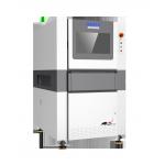
2D Automated Optical Inspection 1.2m online Single-Track Model K2012XL1200 Testing Capability Test items CHIP component body, CHIP component solder ...
2026-10-23 00:42:53
|
|
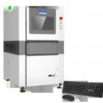
... even the smallest defects, such as shorts, opens, misalignments, and incorrect polarity. The images captured by the camera are processed using ...
2026-10-23 00:42:53
|

|
...AOI features 1. High cost performance 2. Standard 5 million global exposure industrial color camera 3. The first company in China to use large...
2026-10-23 00:42:53
|
|
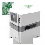
...AOI features 1. High cost performance 2. Standard 5 million global exposure industrial color camera 3. The first company in China to use large...
2026-10-23 00:42:53
|
|
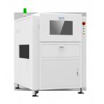
...AOI features 1. High cost performance 2. Standard 5 million global exposure industrial color camera 3. The first company in China to use large...
2026-10-23 00:42:53
|
|
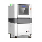
...inspection Features 1.High speed, single FOV processing time is about 350ms 2.Anti-interference, high precision, large range 3.RGB light source ...
2026-10-23 00:42:53
|
|
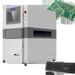
...AOI inspection equipment is designed to provide you with a high-resolution, high-speed inspection solution that can help you detect defects and ...
2026-10-23 00:42:53
|