
21 - 30 of 183
automated wafer inspection machine
Selling leads

|
...LED appearance inspection M2025 Inspection Inspection items Missed bonding, wrong bonding, die damaged, die offset, die tilted, die flipped, wrong ...
2026-10-23 00:42:53
|

|
...-off, poor collinearity Inspection method Image processing, machine learning Optical System Camera 20MP Lens High resolution bi-telecentric lens ...
2026-10-23 00:42:53
|

|
...Defective die removing, residues cleaning, solder paste/adhesive printing, die bonding, solder curing, luminescence inspection Wafer size 3x5mil...
2026-10-23 00:42:53
|

|
...Inspection Equipment is designed to provide maximum inspection accuracy and speed. With high-resolution capabilities, it provides a clear and ...
2026-10-23 00:42:53
|
|
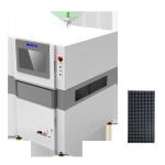
...LED appearance inspection M2012 Inspection Inspection items Missed bonding, wrong bonding, die damaged, die offset, die tilted, die flipped, wrong ...
2026-10-23 00:42:53
|

|
...Automated Optical Inspection Online dual track Model K2005DT Testing Capability Test items CHIP component body, CHIP component solder joints, ...
2026-10-23 00:42:53
|

|
...Automated Optical Inspection Device model K2005DW Detection capacity Detection items CHIP component body, CHIP component solder joints, characters, ...
2026-10-23 00:42:53
|

|
... optical system (light source consistency) 5. High stability integrated casting platform Application scope: solder joint and mounted device ...
2026-10-23 00:42:53
|

|
...Machine comes equipped with a 6.5 Mpix high-speed color camera, providing you with clear and detailed images of your PCBs. The camera has a ...
2026-10-23 00:42:53
|

|
... optical system (light source consistency) 5. High stability integrated casting platform Application scope: solder joint and mounted device ...
2026-10-23 00:42:53
|