
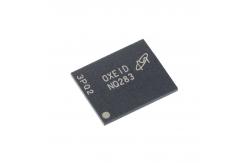
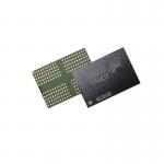
MT29F2G08ABAEAH4-IT:E NAND Flash Memory Ic Chip
|
|
MT29F2G08ABAEAH4-IT:E NAND Flash Asynchronous SLC 2Gbit 8bit 35mA 256MX8 VFBGA-63 Specifications
Description Micron NAND Flash devices include an asynchronous data interface for high-perform-ance I/O operations. These devices use a highly multiplexed 8-bit bus (I/Ox) to transfer commands, address, and data. There are five control signals used to implement the asynchronous data interface: CE#, CLE, ALE, WE#, and RE#. Additional signals control hardware write protection and monitor device status (R/B#). This hardware interface creates a low pin-count device with a standard pinout that re-mains the same from one density to another, enabling future upgrades to higher densi-ties with no board redesign. A target is the unit of memory accessed by a chip enable signal. A target contains one or more NAND Flash die. A NAND Flash die is the minimum unit that can independently execute commands and report status. A NAND Flash die, in the ONFI specification, is referred to as a logical unit (LUN). There is at least one NAND Flash die per chip enable signal. For further details, see Device and Array Organization. This device has an internal 4-bit ECC that can be enabled using the GET/SET features. See Internal ECC and Spare Area Mapping for ECC for more information. Array Addressing – MT29F2G08 (x8) Notes: 1. Block address concatenated with page address = actual page address. CAx = column ad-dress; PAx = page address; BAx = block address. 2. If CA11 is 1, then CA[10:6] must be 0. 3. BA6 controls plane selection. Features • Open NAND Flash Interface (ONFI) 1.0-compliant1 • Single-level cell (SLC) technology • Organization – Page size x8: 2112 bytes (2048 + 64 bytes) – Page size x16: 1056 words (1024 + 32 words) – Block size: 64 pages (128K + 4K bytes) – Plane size: 2 planes x 1024 blocks per plane – Device size: 2Gb: 2048 blocks • Asynchronous I/O performance – tRC/tWC: 20ns (3.3V), 25ns (1.8V) • Array performance – Read page: 25µs 3 – Program page: 200µs (TYP: 1.8V, 3.3V)3 – Erase block: 700µs (TYP) • Command set: ONFI NAND Flash Protocol • Advanced command set – Program page cache mode4 – Read page cache mode 4 – One-time programmable (OTP) mode – Two-plane commands 4 – Interleaved die (LUN) operations – Read unique ID – Block lock (1.8V only) – Internal data move • Operation status byte provides software method for detecting – Operation completion – Pass/fail condition – Write-protect status • Ready/Busy# (R/B#) signal provides a hardware method of detecting operation completion • WP# signal: Write protect entire devic • First block (block address 00h) is valid when ship-ped from factory with ECC. For minimum required ECC, see Error Management. • Block 0 requires 1-bit ECC if PROGRAM/ERASE cycles are less than 1000 • RESET (FFh) required as first command after power-on • Alternate method of device initialization (Nand_Init) after power up (contact factory) • Internal data move operations supported within the plane from which data is read • Quality and reliability – Data retention: 10 years – Endurance: 100,000 PROGRAM/ERASE cycles • Operating voltage range – VCC: 2.7–3.6V – VCC: 1.7–1.95V • Operating temperature – Commercial: 0°C to +70°C – Industrial (IT): –40ºC to +85ºC – Automotive Industrial (AIT): –40°C to +85°C – Automotive (AAT): –40°C to +105°C • Package – 48-pin TSOP type 1, CPL2 – 63-ball VFBGA Trading Guides
|
|||||||||||||||||||||||||||||||||||||||||||||||||||||||
| Product Tags: MT29F2G08ABAEAH4-IT:E Memory Ic Chip MT29F2G08ABAEAH4-IT:E Flash Memory Ic |
|
M24C02-WMN6TP EEPROM EEPROM S I2C 2K 1-Kbit and 2-Kbit serial I²C bus EEPROMs |
|
MTFC4GLWDM-4M 2.7V-3.6V eMMc 4GB 70MB/s read speed 7.5MB/s write speed memory chip |
|
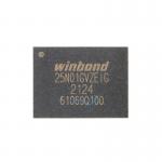
W25N01GVZEIG NAND Flash Memory IC |
|
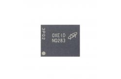
MT29F2G08ABAEAH4-IT:E NAND Flash Memory Ic Chip |
|
SPI Flash Memory IC Chip W25Q128JVPIQ 3V 128M-Bit 16Mx8 133MHz NOR Flash WSON-8 |
|
W25Q80DVZPIG NOR Flash Memory IC Chip 8Mbit 104MHz 2.7V To 3.6V WSON-8 |