
221 - 230 of 230
low resistance gold plated wire
Selling leads

|
... efficiency BGA testing capabilities for semiconductors and SiC wafers. Key Product Features High Conductivity Gold Plating: Gold-plated plunger ...
2025-12-28 00:30:28
|

|
... efficiency BGA testing capabilities for semiconductors and SiC wafers. Key Product Features High Conductivity Gold Plating: Gold-plated plunger ...
2025-12-28 00:30:28
|

|
... efficiency BGA testing capabilities for semiconductors and SiC wafers. Key Product Features High Conductivity Gold Plating: Gold-plated plunger ...
2025-12-28 00:30:28
|

|
... efficiency BGA testing capabilities for semiconductors and SiC wafers. Key Product Features High Conductivity Gold Plating: Gold-plated plunger ...
2025-12-28 00:30:28
|

|
... efficiency BGA testing capabilities for semiconductors and SiC wafers. Key Product Features High Conductivity Gold Plating: Gold-plated plunger ...
2025-12-26 00:28:26
|

|
... efficiency BGA testing capabilities for semiconductors and SiC wafers. Key Product Features High Conductivity Gold Plating: Gold-plated plunger ...
2025-12-26 00:28:26
|

|
... efficiency BGA testing capabilities for semiconductors and SiC wafers. Key Product Features High Conductivity Gold Plating: Gold-plated plunger ...
2025-12-26 00:28:26
|
|
...high efficiency BGA testing capabilities for semiconductors and SiC wafers. Key Product Features High Conductivity Gold Plating: Gold-plated ...
2025-12-26 00:28:26
|

|
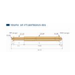
..., Drill Size: 1.4mm, Minimum Test Distance 1.91mm, Full Stroke 2.50mm, Spring Pressure 100g, Current 3A, Resistance 50m Ohm Made of high quality ...
2025-12-25 10:49:18
|

|
...Gold Plating Contact Probe Pins for PCB & ICT Test Product Description Customized ultra-sharp pogo pin ICT test probe pin electronic spring probe ...
2025-12-25 10:49:14
|