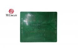
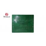
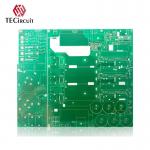
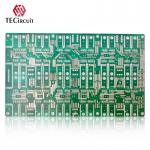
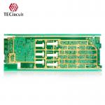
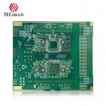
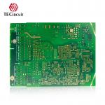
Product Images About TECircuit Found: TECircuit has been operating since 2004.
Location: An electronics manufacturing service(EMS) provider located in
Shenzhen China.
Item: Customizable EMS PCB, offers a full range of one-stop shop services.
Service: Printed Circuit Board (PCB)and Printed Circuit Board Assembly(PCBA), Flexible Printed Circuit Board(FPC), Components Sourcing, Box-Building, Testing.
Quality Assurance: UL,ISO 9001, ISO 14001, ISO 13485, ITAF 16949 andcomplied with ROHS and REACH.
Factory Pictures: Company's own plant : 50,000 sqm; Employees : 930+; Monthly
production capacity : 100,000 m2 Product Applications Medical Devices: Used in equipment such as diagnostic machines and monitoring
systems, where precision and reliability are critical. Test and Measurement Equipment: Essential for devices that require accurate measurements,
including oscilloscopes and signal analyzers. Communication Devices: Integrated into high-frequency communication systems, ensuring
reliable signal transmission and reception. Aerospace and Defense: Utilized in avionics and military applications where performance
and durability are paramount. Industrial Automation: Found in control systems and sensors for machinery, enhancing
operational efficiency and precision. Consumer Electronics: Used in high-performance gadgets that require compact yet
effective circuitry. Automotive Electronics: Employed in advanced driver-assistance systems (ADAS) and other
automotive applications requiring precise control and monitoring. Robotics: Integrated into robotic systems for control and communication,
facilitating complex functions and interactions.
Product Features High Density: Multilayer PCBs allow for complex circuitry in a compact space,
accommodating high-density interconnections essential for precision
instruments. Layered Construction: These boards consist of multiple layers of conductive pathways,
which improve circuit performance and reduce electromagnetic
interference (EMI). Enhanced Signal Integrity: The design minimizes signal loss and crosstalk, ensuring reliable
performance in sensitive applications. Thermal Management: Multilayer PCBs can incorporate thermal vias and heat sinks,
enabling efficient heat dissipation and maintaining optimal
operating temperatures. Durability: Built with robust materials, these PCBs are resistant to
environmental factors such as moisture and temperature
fluctuations, enhancing longevity. Flexibility in Design: The multilayer structure allows for intricate designs and custom
layouts tailored to specific requirements of precision instruments. Improved Reliability: With fewer interconnections needed, multilayer PCBs reduce
potential failure points, increasing overall reliability in
critical applications. Cost-Effectiveness: While initial costs may be higher, multilayer PCBs can lead to
reduced assembly time and lower manufacturing costs in the long
run.
FAQ Question 1: What is needed for a quotation? Answer: PCB: QTY, Gerber file, and Technical Requirements( material/surface
finish treatment/copper thickness/board thickness,...) PCBA: PCB information, BOM,(Testing documents...)
Q2: What file formats do you accept for production? Answer: PCB Gerber file BOM list for PCB Test method for PCBA
Q3: Are my files safe? Answer: Your files are held completely safe and secure. We protect the IP
for our customers in the whole process. All documents from
customers are never shared with any 3rd parties.
Q4: What is the shipment method? Answer: We can offer FedEx /DHL / TNT / UPS for shipment. Also, customer
provided shipment method is acceptable.
Q5: What is the payment method? Answer: Telegraphic Transfer in advance (Advance TT, T/T), PayPal is
acceptable. Product Description Specification: | PCB layers: | 1-42layers | PCB materials: | CEM1, CEM3, Rogers, FR-4, High Tg FR-4, Aluminum Base, Halogen Free | PCB max. board size: | 620mm*1100mm | PCB certificate: | RoHS Directive-Compliant | PCB Thickness: | 1.6 ±0.1mm | Out Layer Copper Thickness: | 0.5-5oz | Inner Layer Copper Thickness: | 0.5-4oz | PCB max. board thickness: | 6.0mm | Minimum Hole Size: | 0.20mm | Minimum Line Width/Space: | 3/3mil | Min. S/M Pitch: | 0.1mm(4mil) | Plate Thickness and Aperture Ratio : | 30:1 | Minimum Hole Copper: | 20µm | Hole Dia. Tolerance(PTH): | ±0.075mm(3mil) | Hole dia. Tolerance(NPTH): | ±0.05mm (2mil) | Hole Position Deviation: | ±0.05mm (2mil) | Outline Tolerance: | ±0.05mm (2mil) | PCB solder mask: | Black, white, yellow | PCB surface finished: | HASL Leadfree,Immersion ENIG,Chem Tin,Flash Gold,OSP,Gold
finger,Peelable,Immersion Silver | Legend: | White | E-test: | 100% AOI, X-ray, Flying probe test. | Outline: | Rout and Score/V-cut | Inspection Standard: | IPC-A-610CCLASSII | Certificates: | UL (E503048),ISO9001/ISO14001/IATF16949 | Outgoing Reports: | Final Inspection, E-test, Solderability Test, Micro Section and
More |
|