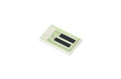
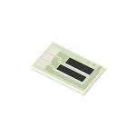
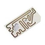
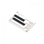
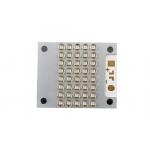
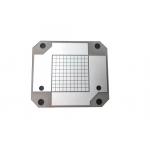
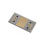
Product Images
About TECircuit Found: TECircuit has been operating since 2004.
Location: An electronics manufacturing service(EMS) provider located in
Shenzhen China.
Item: Customizable EMS PCB, offers a full range of one-stop shop services.
Service: Printed Circuit Board (PCB)and Printed Circuit Board Assembly(PCBA), Flexible Printed Circuit Board(FPC), Components Sourcing, Box-Building, Testing.
Quality Assurance: UL,ISO 9001, ISO 14001, ISO 13485, ITAF 16949 andcomplied with ROHS and REACH.
Factory Pictures:
Company's own plant : 50,000 sqm; Employees : 930+; Monthly
production capacity : 100,000 m2 Product Applications Vision Correction Devices: - Used in advanced eyewear technologies, such as smart glasses that
incorporate vision correction along with digital display features.
Retinal Implants: - Integrated into devices that restore vision by stimulating retinal
cells, providing a solution for patients with severe visual
impairments.
Adaptive Optics Systems: - Employed in systems that adjust optical elements in real-time for
improved imaging quality, often used in advanced diagnostic
equipment.
Surgical Instruments: - Used in precision surgical tools that require reliable electronic
control for procedures involving the eye.
Diagnostic Equipment: - Integrated into devices used for eye examinations and diagnostics,
such as optical coherence tomography (OCT) systems.
Wearable Vision Enhancement Devices: - Used in wearable technology that enhances vision through electronic
means, such as augmented reality applications.
Vision Therapy Systems: - Employed in therapeutic devices designed for vision training and
rehabilitation, integrating sensors and feedback mechanisms.
Smart Contact Lenses: - Integrated into prototype smart contact lenses that monitor health
metrics or provide augmented reality features.
Lighting Systems for Optical Devices: - Used in LED lighting circuits that enhance the performance of
optical instruments, improving visibility and accuracy.
Automated Testing Equipment: - Employed in equipment that tests and calibrates ophthalmic lenses
and devices, ensuring quality and performance standards.
Product Features Biocompatibility: - Designed with materials that are safe for use in medical
applications, particularly those in close contact with human
tissues.
High Thermal Stability: - Ceramic materials provide excellent heat resistance, making them
suitable for environments with varying temperatures.
Mechanical Strength: - Ceramic PCBs are known for their rigidity and durability, ensuring
reliability in delicate applications like ophthalmic devices.
Low Electrical Conductivity: - Helps in minimizing interference in sensitive electronic
applications, maintaining signal integrity.
Lightweight: - Offers a lightweight solution, which is crucial for comfort in
wearable devices like glasses and smart contact lenses.
High Precision: - Manufactured to meet tight tolerances and specifications, ensuring
accurate performance in optical applications.
Resistance to Environmental Factors: - Often treated to resist moisture, dust, and chemicals, enhancing
durability and reliability in various conditions.
Customizability: - Can be tailored to meet specific design and functional
requirements, allowing for innovative ophthalmic solutions.
Ease of Integration: - Designed to accommodate various electronic components, facilitating
seamless integration into complex optical systems.
Compliance with Medical Standards: - Manufactured to meet stringent medical device regulations and
standards, ensuring safety and efficacy in healthcare applications.
FAQ Question 1: What is needed for a quotation?
Answer:
PCB: QTY, Gerber file, and Technical Requirements( material/surface
finish treatment/copper thickness/board thickness,...)
PCBA: PCB information, BOM,(Testing documents...)
Q2: What file formats do you accept for production?
Answer:
PCB Gerber file
BOM list for PCB
Test method for PCBA
Q3: Are my files safe?
Answer:
Your files are held completely safe and secure. We protect the IP
for our customers in the whole process. All documents from
customers are never shared with any 3rd parties.
Q4: What is the shipment method?
Answer:
We can offer FedEx /DHL / TNT / UPS for shipment. Also, customer
provided shipment method is acceptable.
Q5: What is the payment method?
Answer:
Telegraphic Transfer in advance (Advance TT, T/T), PayPal is
acceptable. Product Description | Specification: | | PCB layers: | 1-42layers | | PCB materials: | CEM1, CEM3, Rogers, FR-4, High Tg FR-4, Aluminum Base, Halogen Free | | PCB max. board size: | 620mm*1100mm | | PCB certificate: | RoHS Directive-Compliant | | PCB Thickness: | 1.6 ±0.1mm | | Out Layer Copper Thickness: | 0.5-5oz | | Inner Layer Copper Thickness: | 0.5-4oz | | PCB max. board thickness: | 6.0mm | | Minimum Hole Size: | 0.20mm | | Minimum Line Width/Space: | 3/3mil | | Min. S/M Pitch: | 0.1mm(4mil) | | Plate Thickness and Aperture Ratio : | 30:1 | | Minimum Hole Copper: | 20µm | | Hole Dia. Tolerance(PTH): | ±0.075mm(3mil) | | Hole dia. Tolerance(NPTH): | ±0.05mm (2mil) | | Hole Position Deviation: | ±0.05mm (2mil) | | Outline Tolerance: | ±0.05mm (2mil) | | PCB solder mask: | Black, white, yellow | | PCB surface finished: | HASL Leadfree,Immersion ENIG,Chem Tin,Flash Gold,OSP,Gold
finger,Peelable,Immersion Silver | | Legend: | White | | E-test: | 100% AOI, X-ray, Flying probe test. | | Outline: | Rout and Score/V-cut | | Inspection Standard: | IPC-A-610CCLASSII | | Certificates: | UL (E503048),ISO9001/ISO14001/IATF16949 | | Outgoing Reports: | Final Inspection, E-test, Solderability Test, Micro Section and
More |
|