EL Tester Machine for Solar Modules
Product Description
During the detection process, it does
not directly contact the object under test, so it will not cause
physical damage or interference to the object under test,
maximizing the integrity and original performance of the tested
components. For example, in the detection of photovoltaic modules,
it will not scratch the surface of photovoltaic cells due to
contact. It is very suitable for the detection of some electronic
devices with high requirements for surface quality.
This detection method can also reduce the test errors caused by
contact, making the detection results more accurate and reliable
and truly reflecting the internal condition of the object under
test.
Product Parameters
| Product parameter | Data |
| Shooting Mode | Direct Scanning Method (Modules front facing down, non-lifting
type)Camera is fixed, component is moved for shooting |
| Application Type | Before Lamination/After Lamination |
| Modules Transfer Method | Module is transferred with the long side facing forward (transverse
transfer) |
| No. of Main Busbars | Main Busbar Compatibility:10-20BB |
| Modules Placement Method | Flat |
| Transfer Module Table Height | 950mm (±50mm) |
| Modules Size | Length 1640-2300mm, Width 950-1300mm Regular/Double Glass +
Half-cell (156-159 cells) |
| Test Time | <22 s/pcs (shoot first, then judge) |
| Camera Type | Non-cooling type industrial camera, with a 950nm filter added to
the lens |
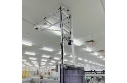
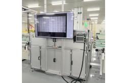
Detailed Photos
camera
Conveyor belt
control button It has high detection sensitivity to tiny defects, electron
concentration changes, injection efficiencies and other parameters
inside the object under test. It can detect small hidden cracks,
fragments, false soldering, broken grids and other defects in solar
cell modules. These defects may affect the performance and service
life of electronic equipment. Through the high-precision detection
of EL testers, they can be detected and dealt with in time.
It has a
high-resolution imaging ability and can clearly present the
internal structure and defect situation of the object under test,
facilitating the observation and analysis by operators. For
example, by using infrared cameras and other imaging components, it
can capture the weak light signals emitted by the object under test
and convert them into clear images.
Company Profile
Beijing X-Solar Energy Co., Ltd.
was found in 2020, and headquartered in Beijing. It's a science and
technology innovative energy enterprises with the main business of
future cell R&D, flexible photovoltaic modules, building
photovoltaic module production, high-end equipment manufacturing,
production line delivery, and AI-CITY wisdom energy management
services.
In
July 2023, the company's first demonstration factory, Jiangsu
X-Solar Green-building Technology Co., Ltd., was established
in Jiangyin CNBM Jetion Industrial Park. Meanwhile,
Jiangsu YuanTeng FengSheng Intelligent Manufacturing Technology
Co., Ltd., a wholly-owned equipment company of the company,
delivered the world's first "three-in-one" automatic production
line for Jiangyin base. The production line can be compatible with
the production of three categories: X-Solar Light
shadow series (flexible PV modules), X-Solar Light
rhyme series (building PVtile modules), X-Solar Light
Curtain series (building PV wall modules), and customized
products. X-Solar PV series products have the advantages
of integrating architectural aesthetics, complying with design
specifications and creating energy value, which have been
widely recognized and praised by customers in domestic and
overseas.
In 2024, the
company has added two regional centers in Shanghai and
Guangzhou of China, and set up the Hong Kong
X-Solar Future Energy Research Institute, and overseas sales
companies in Australia, Italy, Germany, Saudi Arabia and Argentina.
The company has launched a global layout to provide sustainable
energy products and services to many countries, and has contributed
to the "carbon neutrality and carbon peak".
Exhibition Display
FAQ
I. Questions about the principle
Question: What is the working principle of the EL tester?
Answer: The EL tester mainly works based on the
principle of electroluminescence. When a forward bias voltage is
applied to the tested photovoltaic modules, semiconductor devices,
etc., the recombination of carriers inside them will release energy
in the form of light. The EL tester captures the emitted light
through high-sensitivity imaging devices such as cameras, and then
analyzes whether there are defects inside the tested objects and
whether the structure is normal according to the distribution and
intensity of the light.
Question: How does it detect internal defects?
Answer: It relies on detecting the uniformity
and intensity changes of the light signals generated by
electroluminescence of the objects. For example, when a normal
solar cell emits light under power supply, the overall light
intensity distribution is relatively uniform. If there are hidden
cracks, false soldering and other defects, the light intensity at
the defect positions will become weaker or there will be abnormal
dark areas. The EL tester can capture these changes in light
signals and thus detect the defects.
II. Questions about application scenarios
Question: In which fields are EL testers usually used?
Answer: They are mainly applied in the
photovoltaic industry to conduct quality inspections on solar cell
modules and check for problems such as hidden cracks, fragments,
and broken grids. They are also used in the semiconductor industry
to detect the integrity of the internal structure of semiconductor
chips and other devices, as well as the electron injection
efficiency. Meanwhile, they are also used in the inspection of LED
lighting products to check whether there are defective solder
joints and other defects in LED chips.
Question: What can the EL tester be used for at
the photovoltaic power station site?
Answer: At the photovoltaic power station site,
a portable EL tester can be used to quickly detect the installed
photovoltaic modules, check for faults such as hidden cracks and
cell desoldering that may occur during transportation, installation
or after long-term use, timely identify the faulty modules and
arrange for maintenance or replacement to ensure the power
generation efficiency and stable operation of the power station.
III. Questions about detection accuracy
Question: How high is the detection accuracy of the EL tester?
Answer: It can detect tiny hidden cracks at the
micrometer level and very subtle false soldering and other defects.
Some internal structural flaws that are difficult to be found by
the naked eye or even by conventional detection means can be
detected through the high-resolution imaging of the EL tester
combined with precise light signal analysis algorithms. Its
accuracy is sufficient to meet the requirements of most
photovoltaic, semiconductor and other related industries for
component quality control.
Question: How to ensure the stability of the
detection accuracy?
Answer: On the one hand, the optical imaging
system of the tester should be calibrated regularly to ensure that
cameras and other equipment can accurately capture light signals.
On the other hand, the testing environment should be kept
relatively stable, such as light conditions, temperature and
humidity. At the same time, the instrument should be operated in
accordance with standard specifications, and the internal data
processing algorithms should be updated and optimized regularly.
All these help maintain the stability of the detection accuracy.
IV. Questions about operation and use
Question: Is the operation of the EL tester complicated?
Answer: The operation of most EL testers is
relatively simple. There is an intuitive operation interface.
Operators only need to set corresponding basic test parameters such
as voltage and current according to the type and specification of
the tested object, and then start the test. The instrument can
automatically conduct the test and generate test images and
results. Some portable ones can even start the testing process with
just one click.
Question: What should be paid attention to when
using the EL tester for the first time?
Answer: When using it for the first time,
carefully read the user manual to understand the basic functions of
the instrument and the functions of each component. Do a good job
in the installation and commissioning of the instrument, such as
connecting the power cord and data cable to ensure normal
communication and power supply. Also, perform simple initialization
settings for the instrument, such as setting the language and image
display mode. It is best to use standard test samples for testing
practice first to familiarize yourself with the operation process
and result interpretation methods.
V. Questions about maintenance
Question: How to maintain the EL tester on a daily basis?
Answer: Keep the surface of the instrument
clean on a daily basis to avoid dust and other substances from
entering the optical imaging system and affecting the detection
effect. Regularly check whether the cables of the instrument are
damaged and whether the connectors are loose. Use professional
cleaning tools to wipe and clean the lens of the imaging system in
the correct way. Also, regularly check the software version of the
instrument and update and upgrade it in time to obtain better
performance and function optimization.
Question: How to troubleshoot when the
instrument fails?
Answer: First, check whether there is an error
message prompt on the instrument, and judge the general direction
of the fault according to the prompt. For example, if it prompts a
power failure, then check whether the power cord and power adapter
are working normally. If there is a problem with imaging, check the
camera lens, the image transmission line and the relevant image
acquisition software settings. If the software runs abnormally, try
restarting the instrument and the software. If the problem still
cannot be solved, contact the after-sales technical personnel of
the manufacturer for further troubleshooting and repair.
VI. Questions about the interpretation of test results
Question: How to understand the test images generated by the EL
tester?
Answer: Under normal circumstances, the light
intensity distribution in the image is uniform, and the color and
brightness are relatively consistent. If there are darker areas,
striped or blocky abnormal light and shadow, it may indicate that
there are defects at the corresponding positions. For example, dark
lines may indicate hidden cracks, and local dark blocks may
indicate false soldering or cell damage. At the same time, combine
the relevant labels and test data given by the instrument to
comprehensively judge the type and severity of the defects.
Question: What do the various parameters in the
test results represent?
Answer: The light intensity value reflects the
light emission intensity at the corresponding position. The light
intensity uniformity parameter reflects the uniformity of carrier
recombination and light emission inside the tested object. The
closer the value is to 1, the more uniform it is. There are also
parameters such as contrast that can help judge the difference
between the defective area and the normal area. Different
parameters help analyze the quality status of the tested object
from different aspects.