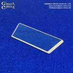
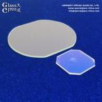
High Clarity Optical Borosilicate Glass Substrates In Semiconductor
Material: Base Composition: Primarily silicon dioxide (SiO₂) and
boron trioxide (B₂O₃) , with minimal alkali content. Manufacturing: Produced via continuous melting in
platinum-lined furnaces to ensure extreme purity and homogeneity.
Often polished to sub-nanometer surface roughness. Key Additives: Precise additions of alumina
(Al₂O₃) for chemical stability and refining
agents to eliminate bubbles/impurities.
Key Properties: Exceptional Optical Clarity: Ultra-high light transmission
(>90%) across UV to NIR spectra (e.g., 185nm-2μm), minimal
autofluorescence. Low Thermal Expansion (CTE): Extremely low CTE (∼3.3 × 10⁻⁶/K
at 20°C), matching silicon wafers to prevent stress-induced failure
during thermal cycling. Superior Thermal & Chemical Resistance: Withstands
aggressive semiconductor processes: Thermal: Stable up to 500°C; resists thermal shock from rapid
heating/cooling. Chemical: Inert to acids, alkalis, and solvents (e.g.,
photoresist developers, etchants).
High Surface Quality: Near-atomic smoothness (<0.5nm Ra)
critical for nanolithography and thin-film deposition. Low Ionic Contamination: Minimal alkali ion migration (Na⁺,
K⁺) prevents device contamination. Mechanical Stability: High Young’s modulus (∼64 GPa) ensures
dimensional rigidity under processing stress.
Primary Function: To serve as an ultra-stable, inert platform for
semiconductor fabrication processes. Provides a defect-free surface for high-resolution
patterning (e.g., EUV photomasks). Acts as a protective window for sensors and optics in
harsh environments. Enables precise light transmission for inspection,
metrology, and lithography systems.
Main Applications in Semiconductor: Photomask Blanks: Base material for EUV/ArF photolithography
masks requiring near-zero defects. MEMS & Sensor Covers: Hermetic sealing caps for pressure
sensors, IR detectors, and MEMS devices. Wafer Handling Components: Carrier plates, inspection windows,
and alignment stages in wafer processing tools. Advanced Packaging: Interposers and substrates for 2.5D/3D IC
integration. Process Equipment Optics: Lenses, viewports, and mirrors in
plasma etchers, CVD chambers, and laser tools. Metrology & Inspection: Critical for high-precision
alignment systems and defect scanners.
In essence: High Clarity Optical Borosilicate Glass Substrates are ultra-pure, thermally stable engineered materials essential
for semiconductor manufacturing. Their unique combination of
near-perfect optical transmission, near-zero thermal expansion,
chemical inertness, and atomic-level surface flatness enables
nanometer-scale precision in photolithography, protects sensitive
components, and ensures reliability in extreme process
environments. These substrates directly support yield and
performance in advanced nodes (e.g., sub-5nm), MEMS production, and
next-generation packaging.
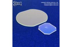
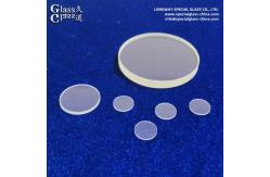
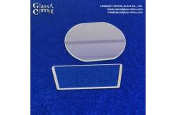
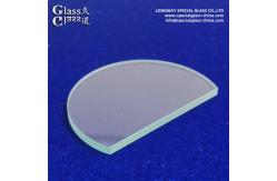
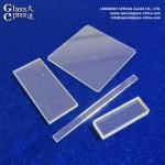
| Item | Glass disc, Glass wafer, Glass substrate | | Material | Optical glass, Qurartz glass, borosilicate glass, Float glass,
borofloat | | Diameter Tolerance | +0/-0.2 mm | | Thickness Tolerance | +/-0.2 mm | | Processed | By Cutting,Grinding,Tempering, Polishing | | Surface Quality | 80/50,60/40,40/20 | | Material Quality | No scratches and air bubble | | Transmission | >90% for visible light | | Chamfer | 0.1-0.3 mm x 45 degree | | Surface Coating | Available | | Usage | Photography, Optics, Lighting system, industrial area. |
|