
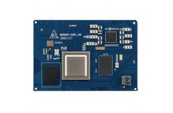
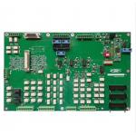
Durable EV Charger PCBA Assembly Suitable For Portable & Stationary Charging Systems
|
|
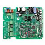
Customizable Durable EV Charger PCBA Assembly Suitable For Portable & Stationary Charging Systems Ring PCB, your PCB & PCBA Turnkey Solutions | Professional Circuit Manufacturing Expert 1. EV Charging Pile PCBA Product Features
Electric Vehicle Charging Pile PCBA Technical Information1. Process Flow
2. Product Features
3. Common Parameters
3.Common technical parameters of EV Charger PCBA common technical parameters for EV Charger PCBA, tailored for an in-house factory offering customization services:
Customization Services Include:
Our vertically integrated factory ensures full control over design, prototyping, and mass production, with lead times optimized for urgent projects. Contact us for tailored solutions!
4. EV Charger PCBA (Printed Circuit Board Assembly) is mainly
applied in the following fields: Why Choose Ring PCB for EV Charger PCBA? At Ring PCB, we don’t just manufacture products—we deliver innovation. With all kinds of PCB Boards, combined with our PCB, PCB Assembly, and turn-key services, we empower your projects to thrive. Whether you need prototyping or mass production, our expert team ensures top-quality results and help you to save money and time. 17 Years of Excellence | Self-Owned Factory | End-to-End Technical
Support Core Advantage 2: Integrated PCBA Services | One-Stop Turnkey
Solutions Core Advantage 3: Self-Owned Factory with Full Supply Chain Control Ring PCB not only offers professional PCB manufacturing, but also offer
PCBA service, including component sourcing and SMT service with
Samsung functional machine. One of our core strengths lies in our 8-stage lead-free reflow soldering and lead-free wave soldering capabilities at our Shenzhen factory. These advanced soldering processes ensure high-quality assembly while adhering to global environmental standards, such as ISO9001, IATF16949 ,RoHS compliance.
Please note:
All products in our store are processing customized services, please be sure to contact our professional customer service before placing an order to confirm the product details. All photos on this site are real. Due to changes in lighting, shooting Angle, and display resolution, the image you see may have some degree of chromatic aberration. Thank you for your understanding. Ring PCB Technology Co.,Limited is a professional PCB manufacturer with 17 years of history in China. Our products are updated and upgraded every year and we specialize in all kinds of PCB making and PCBA customization services, If you are interested in our products, please tell us your requirements, we will help you to provide professional solutions, please contact us on line or E-mail to us info@ringpcb.com, and we will provide you with one-on-one service from our professional sales team. Thank you for your time. |
|||||||||||||||||||||||||||||||||||||||||||||||||||||||||||||||||||||||||||||
| Product Tags: Portable EV Charger PCBA Assembly Stationary EV Charger PCBA Assembly Durable EV Charger PCBA |
|
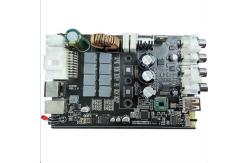
Customizable Electric Vehicle Charging Pile PCBA Full Turnkey Solution With Automated Optical Inspection AOI |
|
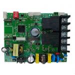
Reliable EV Charger PCBA Supplier , Customizable PCBA Solutions For Bus Automatic Chargers |
|
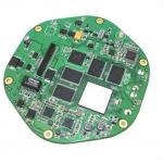
Cost-Effective EV Charger PCBA Professional Manufacturing For Industrial & Public Charging |
|
Electric Vehicle Charging Pile PCBA Assembly with Customizable Durable Design and OSP Surface Finishes |
|
Durable EV Charger PCBA Assembly Suitable For Portable & Stationary Charging Systems |
|
Custom EV Charger PCBA , Fast Turn PCB Assembly For Universal EV Models |