
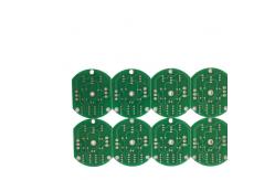
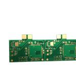
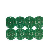
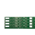
Customization Multilayer PCB Circuit Board HDI And High Density Interconnects
|
Detailed Product Description
FAQ: Question 1.Are you pcba factory? Answer:yes of course. Question 2:Does your factory provide one stop service? Answer:Yes of course we have purchase department and designer. Question 4:can you provide me sample to test before mass order? Answer:Yes of course Question 5:how about your package?are you sure that i will receive the prefect goods without damage? Answer:we provide custom foam box to protect the product.
|
|||||||||||||||||||||||||||||||||||||||||||||||||||||||||||||||||||||||||||||||||||||||||||||||||||||||||||||||
| Product Tags: Customization Multilayer PCB Circuit Board High Density Interconnects PCB Circuit Board Customization multilayer pcb fabrication | |||||||||||||||||||||||||||||||||||||||||||||||||||||||||||||||||||||||||||||||||||||||||||||||||||||||||||||||
Related Products
|
OEM Design Electronic PCB Board Printed Circuit Board With Copper Thickness Of 1oz |
|
Single Sided 94V0 Circuit Board Keyboard PCB Board Osp Surface Finishing Fr4 Base |
|
Customized Silkscreen FR4 PCB Circuit Maker Blind And Buried Vias PCB Boards OEM |
|
Customization Multilayer PCB Circuit Board HDI And High Density Interconnects |
|
Top Notch FR4 PCB Board Electronic PCB Design 1.6mm Thickness |
|
2-16layers FR4 PCB Board For High Performance And Durable Circuits |
Email to this supplier