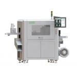
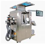
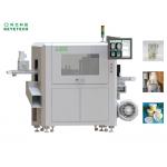
6 Cameras Capacitance Detection Technology: Advanced Multi-Sensor
Imaging for Non-Contact Material Analysis
6 Cameras Capacitance Detection Technology represents a sophisticated approach to non-destructive
testing (NDT) and precision surface characterization, leveraging
the principles of capacitive sensing in a unique multi-sensor array
configuration. This technology employs six highly sensitive "camera-like" capacitive sensor units arranged strategically around the target object. Unlike
optical cameras capturing light, these specialized sensors function
as precision electric field generators and detectors, mapping minute variations in capacitance caused by the target's
inherent electrical properties.
The core principle relies on the interaction between an applied
electric field and the target material. Each "camera" emits a
controlled electric field. When this field encounters the target
object – be it a conductor, semiconductor, or dielectric material
(like polymers, coatings, ceramics, or composites) – it induces
measurable changes in capacitance. These changes are exquisitely
sensitive to critical factors including:
Material Composition and Properties: Differences in dielectric constant or conductivity.
Geometric Features: Surface topography, shape, and proximity.
Thickness Variations: In films, coatings, or layered structures.
Subsurface/Internal Features: Voids, inclusions, delamination, porosity, or density
variations.
The deployment of six synchronized sensors is the key differentiator. This multi-perspective setup
enables:
Comprehensive Field Coverage: Capturing data from multiple angles eliminates blind spots
inherent in single-sensor systems.
Enhanced Spatial Resolution: Combining data streams creates a higher-resolution map of the
object's electrical properties.
Improved Signal-to-Noise Ratio (SNR): Correlating signals from multiple sensors helps distinguish
true material variations from environmental noise.
Volumetric Data Acquisition: Effectively builds a 3D representation of the target's
capacitance profile, revealing both surface and near-subsurface
characteristics.
Faster Scanning: Parallel data acquisition significantly speeds up inspection
compared to sequential scanning methods.
The output is processed using advanced algorithms to generate
intuitive visualizations such as high-resolution capacitance maps, 3D topography reconstructions,
thickness distribution profiles, and defect location overlays. This provides quantifiable insights far beyond simple
proximity detection.
6 Cameras Capacitance Detection Technology excels in scenarios
where contact is undesirable, materials are opaque to light, or
internal features need scrutiny without radiation. Its primary advantages include:
Non-Contact & Non-Destructive: Safely analyzes delicate or sensitive surfaces.
Material Agnostic: Works on conductors, semiconductors, and insulators.
Subsurface Sensitivity: Detects flaws hidden beneath surfaces.
High Resolution & Precision: Reveals minute variations and defects.
Speed & Efficiency: Multi-sensor design enables rapid scanning.
This makes it invaluable for critical applications across
industries:
Semiconductor Manufacturing: Wafer warpage/bow mapping, thin film thickness/uniformity,
package delamination/voiding.
Advanced Materials: Composite layup integrity (fiber orientation, resin pockets,
delamination), coating/adhesive uniformity and thickness.
Battery Production: Electrode coating consistency, separator defects, layer
alignment.
Precision Engineering: Surface finish verification, micro-defect detection,
gap/clearance measurement.
Automotive/Aerospace: Inspection of bonded structures, paint/coating quality,
composite part integrity.
6 Cameras Capacitance Detection Technology transforms complex electrical interactions into actionable,
high-fidelity visual data, providing engineers and quality control
professionals with an unparalleled tool for material insight,
process optimization, and defect prevention in demanding industrial
environments.