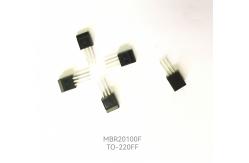
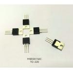
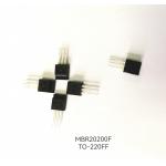
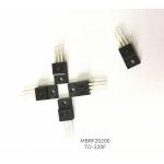
High Current Resistance Schottky Diode For High Frequency Switch
Power Supply
MBR20100.pdf
The internal circuit structure of a typical Schottky rectifier is
based on an N-type semiconductor substrate, on which an N-epitaxial
layer with arsenic as a dopant is formed. The anode uses materials
such as molybdenum or aluminum to make the barrier layer. Silicon
dioxide (SiO2) is used to eliminate the electric field in the edge
area and improve the withstand voltage value of the tube. The
N-type substrate has a very small on-state resistance, and its
doping concentration is 100% higher than that of the H-layer. An N+
cathode layer is formed under the substrate to reduce the contact
resistance of the cathode. By adjusting the structural parameters,
a Schottky barrier is formed between the N-type substrate and the
anode metal, as shown in the figure. When a forward bias is applied
to both ends of the Schottky barrier (the anode metal is connected
to the positive pole of the power supply, and the N-type substrate
is connected to the negative pole of the power supply), the
Schottky barrier layer becomes narrower and its internal resistance
becomes smaller; otherwise, if When a reverse bias is applied to
both ends of the Schottky barrier, the Schottky barrier layer
becomes wider and its internal resistance becomes larger.
Features
1. Common cathode structure
2. Low power loss, high efficiency
3. High Operating Junction Temperature
4. Guard ring for overvoltage protection,High reliability
5. RoHS product
Applications
1. High frequency switch Power supply
2. Free wheeling diodes, Polarity protection applications
ABSOLUTE RATINGS (Tc=25°C)
Parameter | Symbol | Value | Unit |
Repetitive peak reverse voltage | | | |
Maximum DC blocking voltage | | | |
Average forward current | TC=150°C (TO-220/263/252 )TC=125°C(TO-220F) | per device per diode | | | |
Surge non repetitive forward current 8.3 ms single
half-sine-wave (JEDECMethod) | | | |
Maximum junction temperature | | | |
Storage temperature range | | | |