
Very High Accuracy And Stability TSZ121ICT TSZ121 Amplifiers IC 1CIRC SC70-5
|
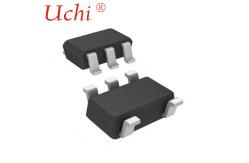
Very high accuracy and stability TSZ121ICT TSZ121 Amplifiers IC OPAMP ZERO-DRIFT 1CIRC SC70-5
Very high accuracy (5 µV) zero drift micropower 5 V operational amplifiers Features Very high accuracy and stability: offset voltage 5 µV max at 25 °C, 8 µV over full temperature range (-40 °C to 125 °C) Rail-to-rail input and output Low supply voltage: 1.8 - 5.5 V Low power consumption: 40 µA max. at 5 V Gain bandwidth product: 400 kHz High tolerance to ESD: 4 kV HBM Extended temperature range: -40 to 125 °C Micro-packages: SC70-5, DFN8 2x2, and QFN16 3x3 Benefits
TSZ121 is the single version, TSZ122 the dual version, and TSZ124
the quad version, with pinouts compatible with industry standards. Absolute maximum ratings and operating conditions Table 1: Absolute maximum ratings (AMR)
Notes: (1)All voltage values, except the differential voltage are with respect to the network ground terminal. (2)The differential voltage is the non-inverting input terminal with respect to the inverting input terminal. (3)Vcc - Vin must not exceed 6 V, Vin must not exceed 6 V (4) Input current must be limited by a resistor in series with the inputs. (5) Rth are typical values. (6)Short-circuits can cause excessive heating and destructive dissipation. (7) Human body model: 100 pF discharged through a 1.5 kΩ resistor between two pins of the device, done for all couples of pin combinations with other pins floating. (8)Machine model: a 200 pF cap is charged to the specified voltage, then discharged directly between two pins of the device with no external series resistor (internal resistor < 5 Ω), done for all couples of pin combinations with other pins floating. (9)Charged device model: all pins plus package are charged together to the specified voltage and then discharged directly to ground.
Table 2: Operating conditions
3
Electrical characteristics Table 3: Electrical characteristics at VCC+ = 1.8 V with VCC- = 0 V, Vicm = VCC/2, T = 25 ° C, and RL = 10 kΩ connected to VCC/2 (unless otherwise specified)
TSZ121, TSZ122, TSZ124 Notes: (1)SeeSection 5.5: "Input offset voltage drift over temperature". Input offset measurements are performed on x100 gain configuration. The amplifiers and the gain setting resistors are at the same temperature. (2)Guaranteed by design (3)Slew rate value is calculated as the average between positive and negative slew rates. Table 4: Electrical characteristics at VCC+ = 3.3 V with VCC- = 0 V, Vicm = VCC/2, T = 25 ° C, and RL = 10 kΩ connected to VCC/2 (unless otherwise specified)
Table 5: Electrical characteristics at VCC+ = 5 V with VCC- = 0 V, Vicm = VCC/2, T = 25 ° C, and RL = 10 kΩ connected to VCC/2 (unless otherwise specified)
Notes: See Section 5.5: "Input offset voltage drift over temperature". Input offset measurements are performed on x100 gain configuration. The amplifiers and the gain setting resistors are at the same temperature. (2)Guaranteed by design (3)Tested on SC70-5 package (4)Slew rate value is calculated as the average between positive and negative slew rates. IMPORTANT NOTICE – PLEASE READ CAREFULLY
STMicroelectronics NV and its subsidiaries (“ST”) reserve the right to make changes, corrections, enhancements, modifications , and improvements to ST products and/or to this document at any time without notice. Purchasers should obtain the latest relevant information on ST products before placing orders. ST products are sold pursuant to ST’s terms and conditions of sale in place at the time of order acknowledgement.
Purchasers are solely responsible for the choice, selection, and use of ST products and ST assumes no liability for application assistance or the design of Purchasers’ products.
No license, express or implied, to any intellectual property right is granted by ST herein.
Resale of ST products with provisions different from the information set forth herein shall void any warranty granted by ST for such product.
ST and the ST logo are trademarks of ST. All other product or service names are the property of their respective owners.
Information in this document supersedes and replaces information previously supplied in any prior versions of this document.
© 2016 STMicroelectronics – All rights reserved For more details, see the specifications in the link
|
|||||||||||||||||||||||||||||||||||||||||||||||||||||||||||||||||||||||||||||||||||||||||||||||||||||||||||||||||||||||||||||||||||||||||||||||||||||||||||||||||||||||||||||||||||||||||||||||||||||||||||||||||||||||||||||||||||||||||||||||||||||||||||||||||||||||||||||||||||||||||||||||||||||||||||||||||||||||||||||||||||||||||||||||||||||||||||||||||||||||||||||||||||||||||||||||||||||||||||||||||||||||||||||||||||||||||||||||||||||||||||||||||||||||||||||||||||||||||||||||||||||||||||||||||||||||||||||||||||||||||||||||||||||||||||||||||||||||||||||||||||||||||||||||||||||||||||||||||||||||||||||||||||||||||||||||||||||||||||||||||||||||||||||||||||||||||||||||||||||||||||||||||||||||||||||||||||||||||||||||||
| Product Tags: TSZ121ICT Amplifiers IC TSZ121 Amplifiers IC SC70-5 ZERO DRIFT OP AMP | |||||||||||||||||||||||||||||||||||||||||||||||||||||||||||||||||||||||||||||||||||||||||||||||||||||||||||||||||||||||||||||||||||||||||||||||||||||||||||||||||||||||||||||||||||||||||||||||||||||||||||||||||||||||||||||||||||||||||||||||||||||||||||||||||||||||||||||||||||||||||||||||||||||||||||||||||||||||||||||||||||||||||||||||||||||||||||||||||||||||||||||||||||||||||||||||||||||||||||||||||||||||||||||||||||||||||||||||||||||||||||||||||||||||||||||||||||||||||||||||||||||||||||||||||||||||||||||||||||||||||||||||||||||||||||||||||||||||||||||||||||||||||||||||||||||||||||||||||||||||||||||||||||||||||||||||||||||||||||||||||||||||||||||||||||||||||||||||||||||||||||||||||||||||||||||||||||||||||||||||||

|
STM32 CTEC ARM Based 32 Bit MCU CKS32F030 Integrated Circuit |
|
Low Power Loss Schottky Diodes High Efficiency High Current Resistance |
|
High Switching Frequency Schottky Diodes , Low Power Loss Free Wheeling Diodes |
|
Strong Ability To Withstand Surge Current Schottky Diodes High Switching Frequency |
|
RoHS Approved Schottky Diode Guard Ring For Overvoltage Protection |
|
High Current Resistance Schottky Diode For High Frequency Switch Power Supply |