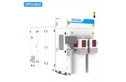
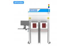
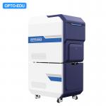
- Compatible With 6/8 Inch Wafers Size, Magnification 1000x-300000x
- Resolution 2.5nm (Acc=800V), Accelerating Voltages 500V--1600V
- Repeatability Static & Dynamic ±1% or 3nm(3 Sigma), Probe Beam
Current 3~30pA
- High-Speed Wafer Transfer System Design Suitable For 3rd-Generation
Semiconductor Chips
- Advanced Electron Optics Systems And Image Processing, Including
Chiller, Dry pump
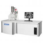
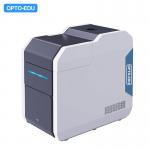
A Critical Dimension Scanning Electron
Microscope (CD-SEM) is a specialized SEM used to measure the
dimensions of tiny features on semiconductor wafers, photomasks,
and other materials. These measurements are crucial for
ensuring the accuracy and precision of manufactured electronic
devices. ◉ Compatible With 6/8 Inch Wafers Size, Magnification 1000x-300000x ◉ Resolution 2.5nm (Acc=800V), Accelerating Voltages 500V--1600V ◉ Repeatability Static & Dynamic ±1% or 3nm(3 Sigma), Probe Beam
Current 3~30pA ◉ High-Speed Wafer Transfer System Design Suitable For 3rd-Generation
Semiconductor Chips ◉ Advanced Electron Optics Systems And Image Processing, Including
Chiller, Dry pump |
▶ Key Features CD-SEMs use a low-energy electron beam and have enhanced
magnification calibration to ensure accurate and repeatable
measurements. They are designed to measure features like the
width, height, and sidewall angles of patterns. |
▶ Purpose CD-SEMs are essential for metrology in the semiconductor industry,
helping to measure the critical dimensions (CDs) of patterns
created during lithography and etching processes. CDs refer to
the smallest feature sizes that can be reliably produced and
measured on a wafer. |
▶ Applications These instruments are used in the manufacturing lines of electronic
devices to ensure the dimensional accuracy of the various layers
and features that make up a chip. They also play a crucial
role in process development and control, helping to identify and
correct any issues that may arise during the manufacturing
process. ▶ Importance Without CD-SEMs, modern microelectronics would struggle to achieve
the high level of precision and performance that is demanded by the
industry. They are indispensable for ensuring the reliability
and functionality of modern electronic devices. |
▶ Shifting Technology As lithography techniques advance and feature sizes continue to
shrink, CD-SEMs are constantly evolving to meet the demands of the
industry. New technologies and advancements in CD-SEM are
being developed to address the challenges of measuring increasingly
complex patterns |
| A63.7190 Critical Dimension Scanning Electron Microscope (CDSEM) | | Wafer Size | A63.7190-68: 6/8 Inches | A63.7190-12: 12 Inches | | Resolution | 2.5nm (Acc=800V) | 1.8nm (Acc-800V) | | Accelerating Voltages | 0.5-1.6KV | 0.3-2.0KV | | Repeatability | Static & Dynamic ±1% or 3nm(3 Sigma) | Static & Dynamic ±1% or 0.3nm(3 Sigma) | | Probe Beam Current | 3~30pA | 3~40pA | | Measuring Range | FOV 0.1~2.0μm | FOV 0.05~2.0μm | | Throughput | >20 Wafers/Hour, | >36 Wafers/Hour, | | 1 Point/Chip, | 1 Point/Chip, | | 20 Chips/Wafer | 20 Chips/Wafer | | Magnification | 1Kx~300Kx | 1Kx-500Kx | | Stage Accuracy | 0.5μm | | Electron Source | Schottky Thermal Field Emitter |
| Comparation of Main CDSEM Models on Market | | Specification | Hitachi | Hitachi | Hitachi | Opto-Edu | Opto-Edu | | S8840 | S9380 | S9380 II | A63.7190-68 | A63.7190-12 | | 1. Wafer Size | 6inch/8inch | 8inch/12inch | 8inch/12inch | 6inch/8inch | 12inch | | 2. Resolution | 5nm (Acc=800V) | 2nm (Acc=800V) | 2nm (Acc=800V) | 2.5nm (Acc=800V) | 1.8nm (Acc=800V) | | 3. Accelerating Voltage | 500-1300V | 300-1600V | 300-1600V | 500-1600V | 300-2000V | | 4. Repeatability (static and dynamic) | ±1% or 5nm(3 sigma) | ±1% or 2nm(3 sigma) | ±1% or 2nm(3 sigma) | ±1% or 3nm(3 sigma) | ±1% or 0.3nm(3 sigma) | | 5. Ip Range (Probe current) | 1-16pA | 3-50pA | 3-50pA | 3-30pA | 3-40pA | | 6. FOV Size | - | 50nm-2um | 0.05-2um | 0.1-2um | 0.05-2um | | 7.Througput | 26 wafers/hour, | 24 wafers/hour, | 24 wafers/hour, | >20wafers/hour, | 36 wafers/hour, | | 1point/chip, | 1point/chip, | 1point/chip, | 1point/chip, | 1point/chip, | | 5chips/wafer | 20chips/wafer | 20chips/wafer | 20chips/wafer | 20chips/wafer |
|