
2-Layer F4BME217 PCB 1.0mm Core PTFE laminate with Bare Copper Finish for RF and microwave
|


|
2-Layer F4BME217 PCB | 1.0mm Core | Bare Copper Finish
Product Overview We are pleased to present this newly customized 2-layer rigid PCB built on Wangling's F4BME217 high-performance PTFE composite laminate. Engineered for demanding RF and microwave applications, this board delivers superior electrical properties, low loss, and excellent passive intermodulation (PIM) performance.
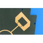
The board measures 102mm x 83mm (single piece) with a finished thickness of 1.3mm (including 1.0mm core + 2 x 35μm copper) and dimensional tolerance of ±0.15mm. Minimum trace and space are 5/6 mils, with a minimum finished hole size of 0.25mm. No blind vias are used in this construction.
A key feature of this design is the bare copper surface finish—no solder mask and no silkscreen on either side. This intentional choice eliminates parasitic losses and ensures optimal RF performance. The F4BME217 material features reverse-treated foil (RTF) copper, which provides superior low-PIM performance (≤-159 dBc), enables precise etching for fine-line circuits, and reduces conductor loss. Every board undergoes 100% electrical testing prior to shipment and conforms to IPC-Class-2 quality standards. Gerber files are supplied in RS-274-X format, and worldwide shipping is available.
PCB General Specifications
Material Advantages: F4BME217 The F4BME217 from Taizhou Wangling Insulation Material Factory is a high-performance PTFE composite laminate precision-formulated from woven fiberglass cloth, PTFE resin, and PTFE film. This next-generation material significantly outperforms earlier grades, offering lower dielectric loss, higher insulation resistance, and enhanced stability. It serves as a reliable, high-performance domestic substitute for comparable imported laminates.
F4BME217 specifically features reverse-treated foil (RTF) copper, which provides three critical advantages for high-frequency designs:
Superior low-PIM performance (≤-159 dBc) – ideal for sensitive communications systems
More precise etching – enabling fine-line circuit patterns
Reduced conductor loss – maintaining signal integrity at high frequencies
The material properties are precisely tuned by adjusting the ratio of PTFE to fiberglass cloth. A higher dielectric constant is achieved by increasing the fiberglass content, which simultaneously improves dimensional stability, lowers the coefficient of thermal expansion, and reduces temperature drift. This design flexibility enables engineers to select the optimal material grade for the perfect balance of electrical performance, mechanical robustness, and processing requirements.
F4BME217 Material Properties
PCB Stackup & Construction The board features a straightforward yet robust 2-layer stackup:
Top Copper (Layer 1): 1 oz (35μm) – RTF copper
Dielectric Core: F4BME217 – 1.0 mm (39.37 mils)
Bottom Copper (Layer 2): 1 oz (35μm) – RTF copper
Total Finished Thickness: 1.3 mm
Minimum trace and space are 5/6 mils, with a minimum finished hole size of 0.25mm. Via plating thickness is 20μm, and no blind vias are used. The design supports 15 components, 42 total pads (17 thru-hole, 25 top SMT), 28 vias, and 7 nets.
Typical Applications Microwave, RF, and Radar systems Phase shifters and passive components Power dividers, couplers, and combiners Feed networks and phased array antennas Satellite communication systems Base station antennas
Additional Capabilities from Wangling The F4BME series also supports aluminum-backed (F4BME*-AL)** and copper-backed (F4BME*-CU)** constructions for shielding or heat dissipation requirements. Standard panel sizes include 460×610mm, 500×600mm, 850×1200mm, 914×1220mm, and 1000×1200mm, with custom dimensions available upon request.
All PCBs are 100% electrically tested and shipped with a Certificate of Conformance per IPC-6012. For Gerber review, stackup confirmation, or volume pricing, please contact our technical sales team.
|
|
2-Layer F4BME217 PCB 1.0mm Core PTFE laminate with Bare Copper Finish for RF and microwave |

|
High DK 10.2 2-Layer F4BTMS1000 PCB built on 10mil substarte laminate with OSP Finish |

|
F4BTMS1000 High Frequency PCB High DK10.2 PTFE 3.2mm Substrates with Immersion Gold |

|
F4BM300 High Frequency PCB 0.6mm PTFE substrates 2oz Copper With Immersion Gold |

|
F4BTM320 High Frequency PCB 2oz Copper 1.27mm Substrates With Immersion Gold |

|
F4BTMS615 High Frequency PCB 1.6mm DK6.15 F4B Substrate With Immersion Gold |