
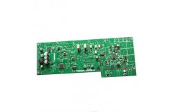
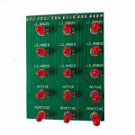
6 Layers Prototype Circuit Board PCBA Board Assembly With High Speed Quickturn
|
|
6 Layers Prototype Circuit Board PCBA Board Assembly With High Speed Quickturn
Files Requested For PCB Assembly Quotation
Production Details
1. Material Management
Supplier → Components Purchase → IQC → Protection Control → Material Supply → Firmware
2. Program Management
PCB Files → DCC → Program Organizing → Optimization → Checking
3. SMT Management
PCB Loader → Screen Printer → Checking → SMD Placement → Checking → Air Reflow → Vision Inspection → AOI → Keeping
4. PCBA Management
THT→Soldering Wave (Manual Welding) → Vision Inspection → ICT → Flash → FCT → Checking → Package → Shipment
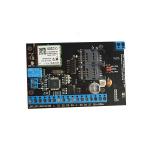
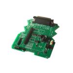
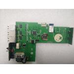
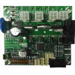
Shinelink kinds PCBA Products
FAQ:
1. What’s the typical process flow for multi-layer PCB? Material cutting → Inner dry film → inner etching → Inner AOI → Multi-bond→ Layer stack up Pressing → Drilling → PTH → Panel Plating → Outer Dry Film → Pattern Plating → Outer etching → Outer AOI → Solder Mask → Component Mark → Surface finish → Routing → E/T → Visual Inspection.
Key equipment list is as following: Laser drilling machine, Pressing machine, VCP line, Automatic Exposing machine, LDI and etc. The equipments we have are the best in the industry, laser drilling machines are from Mitsubishi and Hitachi, LDI machines are from Screen(Japan), Automatic Exposing machines are also from Hitachi, all of them make we can meet customer’s technical requirements.
O-the leader has the full series of surface finish, such as: ENIG, OSP, LF-HASL, gold plating (soft/hard), immersion silver, Tin, silver plating, immersion tin plating, carbon ink and etc. .. OSP, ENIG, OSP + ENIG commonly used on the HDI, we usually recommend that you use a client or OSP OSP + ENIG if BGA PAD size less than 0.3 mm. |
|||||||||||||||||||||||||||||||||||||||||||||||||||||||||||||
| Product Tags: pcb board assembly pcb assembly services |

|
Electronic Custom PCBA Printed Circuit Board Assembly Schematic Diagram Services |
|
Free Sample One Stop Printed Circuit Board Assembly Electronic PCBA Service |
|
SMT Printed Circuit Board Assembly PCB Assembly Service PCBA Manufacturer |
|
SMT PCBA Printed Circuit Board Assembly Quick Turn Prototype And Mass Production |
|
Customized EMS PCBA Board Assembly Electronics Components 1OZ Copper Thickness |
|
Rigid 1oz Copper PCBA Board Assembly PCB 2 Layer ODM PCBA Immersion Gold |