
GaSb
|
|
2-6 inch Gallium phosphide (GaP) crystals crystal substrate,GaP wafer
ZMKJ can provides high quality single crystal GaP wafer ( Gallium phosphide ) to electronic and optoelectronic industry in diameter up to 2 inch . Gallium phosphide ( GaP ) crystal is an orange-yellow semi-translucent material formed by two elements , Gallium and Phosphide , growth by Liquid Encapsulated Czochralski ( LEC ) method . GaP wafer is an important semiconductor material which have unique electrical properties as other III-V compound materials and is widely used as red , yellow , and green LED ( light-emitting diodes ) . We have as-cut single crystal GaP wafer for your LPE application , and also provide epi ready grade GaP wafer for your MOCVD & MBE epitaxial application . Please contact us for more product information .
Electrical and Doping Specification
Product Specification
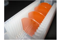
Sample pictures
FAQ: Q: What's the delivery time? A: (1) For the standard products For inventory: the delivery is 5 workdays after you place the order. For customized products: the delivery is 2 or 3 weeks after you place the order. (2) For the special-shaped products, the delivery is 4 workweeks after you place the order. Q: What's your MOQ? A: (1) For inventory, the MOQ is 3pcs. (2) For customized products, the MOQ is 10-20pcs up.
we also can provide other materials semiconductor wafer as like below |
||||||||||||||||||||||||||||||||||||||||||||||||||||||||||||||||||
| Product Tags: mgo substrate gap wafer | ||||||||||||||||||||||||||||||||||||||||||||||||||||||||||||||||||

|
Copper Heat Sink Substrate Flat Bottom Pin Type High Power Electronic Device Cu≥99.9% |

|
InAs Indium Arsenide2inch 3inch 4inch Single Crystal Substrate N/P Type Semiconductor Wafer Thickness 300-800um |

|
Magnesium Oxide Purity 95% MgO Film Substrate 5x5 10x10 20x20 Thickness 0.5mm 1.0mm Orientation <001> <110> <111> |

|
Germanium Substrate GE Flat Windows Optical Lenses Thermal Imaging Applications And Infrared Spectroscopy High Hardness |

|
Ge Germanium Wafer Semiconductor Substrates <111> Concentrating Photovoltaic CPV Custom Size Shapes |

|
InAs Wafer Doped Zn 2 Inch Indium Arsenide Wafer Dia 50mm Thickness 500um <100> Customized |