
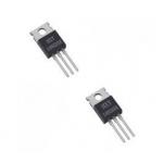
HXY4466 30V Mos Field Effect Transistor N Channel VGS 10V Low Noise
|

|
60V N-Channel AlphaSGT HXY4264
Product Summary
General Description
The HXY4466 uses advanced trench technology to provide excellent RDS(ON) and low gate charge. This device is suitable for use as a load switch or in PWM applications. The source leads are separated to allow a Kelvin connection to the source, which may be used to bypass the source inductance.
Electrical Characteristics (T =25°C unless otherwise noted)
A. The value of RθJA is measured with the device mounted on 1in2 FR-4 board with 2oz. Copper, in a still air environment with TA =25°C. The value in any given application depends on the user's specific board design. B. The power dissipation PD is based on TJ(MAX)=150°C, using ≤ 10s junction-to-ambient thermal resistance. C. Repetitive rating, pulse width limited by junction temperature TJ(MAX)=150°C. Ratings are based on low frequency and duty cycles to keep initialT =25°C. D. The RθJA is the sum of the thermal impedance from junction to lead RθJL and lead to ambient. E. The static characteristics in Figures 1 to 6 are obtained using <300µs pulses, duty cycle 0.5% max. F. These curves are based on the junction-to-ambient thermal impedance which is measured with the device mounted on 1in2 FR-4 board with 2oz. Copper, assuming a maximum junction temperature of TJ(MAX)=150°C. The SOA curve provides a single pulse rating. G. The spike duty cycle 5% max, limited by junction temperature TJ(MAX)=125°C.
TYPICAL ELECTRICAL AND THERMAL CHARACTERISTICS
|
||||||||
| Product Tags: logic mosfet switch mosfet driver using transistor |
|
60N06HX 60V Mos Field Effect Transistor N Channel Enhancement Mode MOSFET |
|
60N03PIT 30V N Channel Mosfet Transistor , High Power Transistor |
|
50N06P/T 60V Mos Field Effect Transistor Silicon Material Junction Temperature 150℃ |
|
G40N10 100V Mosfet Power Transistor , N Channel Transistor Fast Switching |
|
18N20X 200V Mos Field Effect Transistor Low Gate Charge For Switching Application |
|
2N7002 Enhancement Mode Field Effect Transistor VDSS 20v ID 6.0 A |