
251 - 260 of 271
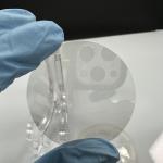
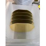
inp crystal semiconductor substrate
Selling leads
|
...substrate wafers. Our wafers are optimal for electronic devices with high power and high frequency, as well as for light emitting diodes (LED). The ...
2025-07-20 00:12:23
|
|
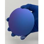
...wafers refers to a substrate material composed of a sapphire substrate with a layer of gallium nitride (GaN) grown on top. GaN is a semiconductor ...
2025-05-06 20:44:26
|
|
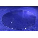
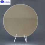
...Substrate DSP/SSP Polished Sapphire Wafer Lens for sale Sapphire Optical Custom-made High Precision Transparent Sapphire Glass Optical Window/Wafer ...
2025-05-06 20:38:05
|
|
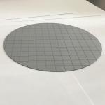
2inch 3inch 4inch 5inch 6inch 8inch 12inch FZ CZ N-type polished silicon wafer DSP SiO2 wafers Silicon oxide wafer 1inch 2inch 10x10mm Scanning ...
2025-05-06 20:44:47
|
|
6inch 8inch 2inch 1inch FZ CZ N-type polished silicon wafer DSP SiO2 wafers Silicon oxide wafer Polished Silicon Wafer High-purity (11N) 1-12 inch ...
2025-05-06 20:44:51
|
|
custom 0.2mm~2mm bf33 glass sheet/borofloat 33 glass sheet High Temperature Resistance BF33/Fused Silica/Sapphire UV/IR Wavelength Optical Glass Sheet...
2025-05-06 20:44:53
|

|
SapphiLarge Thickness Thermal Oxide (SiO2) On Silicon Wafers For Optical Communication System Generally, the oxide layer thickness of silicon wafers ...
2025-07-20 00:12:23
|
|
*, *::before, *::after {box-sizing: border-box;}* {margin: 0;}html, body {height: 100%;}body {line-height: 1.5;-webkit-font-smoothing: antialiased;...
2025-05-06 20:45:05
|
|
N-type SiC on Si Compound Wafer 6inch 150mm SiC type 4H-N Si type N or P N-type SiC on Si Compound Wafer abstract N-type silicon carbide (SiC) on ...
2025-05-06 20:45:18
|
|
*, *::before, *::after {box-sizing: border-box;}* {margin: 0;}html, body {height: 100%;}body {line-height: 1.5;-webkit-font-smoothing: antialiased;...
2025-05-06 20:45:31
|