
201 - 210 of 271
inp crystal semiconductor substrate
Selling leads
|
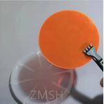
...semiconductor substrate primarily used in the fabrication of various electronic and optoelectronic devices. Gallium Phosphide (GaP) wafers exhibit ...
2025-05-06 20:45:06
|
|
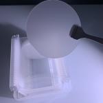
..., optoelectronic devices, semiconductor devices, and other fields. The high light transmittance and high hardness of sapphire wafers make them ...
2025-07-19 00:11:40
|
|
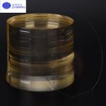
LNOI Wafer 2/3/4/6/8 Inch (Si/LiNbO₃, Customizable) photonic devices Introduce of LNOI Wafer LiNbO3 Crystals is widely used as frequency doublers for ...
2025-06-23 17:12:58
|
|
...semiconductor industry's high demands for purity and performance. These wafers are made from pure raw materials and optimized growth processes, ...
2025-05-06 20:45:04
|
|
...purity and exceptional uniformity, ideal for a wide range of semiconductor and photovoltaic applications. With precise control over crystal ...
2025-05-06 20:45:12
|
|
...crystal (sic) substrates wafersS/ High purity un-doped 4H-semi resistivity>1E7 3inch 4inch 0.35mm sic wafers About Silicon Carbide (SiC)Crystal ...
2025-05-06 20:40:51
|
|
... carbon chips for optical About Silicon Carbide (SiC)Crystal Silicon carbide (SiC), also known as carborundum, is a semiconductor containing ...
2025-05-06 20:40:52
|
|
... wafers silicon carbon chips for optical About Silicon Carbide (SiC)Crystal Silicon carbide (SiC), also known as carborundum, is a semiconductor ...
2025-05-06 20:40:52
|
|
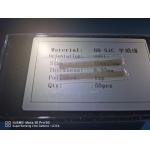
... single crystal (sic) substrates wafersS/ Customzied as-cut sic wafersProduction 4inch grade 4H-N 1.5mm SIC Wafers for seed crystal About Silicon ...
2025-05-06 20:40:54
|
|
... as the foundation for high-performance semiconductor devices. Crafted with advanced float-zone mono-crystalline silicon technology, this substrate ...
2025-05-06 20:45:11
|