
201 - 210 of 281
dsp windows substrate wafer
Selling leads
|
Product Description: Our InP (Indium Phosphide) wafers are renowned for their low defect density and high performance, widely used in optoelectronics ...
2025-05-06 20:44:24
|
|
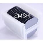
Silicon Wafer CZ orientation111 Resistivity: 1-10 (ohm.cm) single side or double side polish Product abstract Our Si wafer offers high purity and ...
2025-05-06 20:45:12
|
|
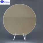
N-type SiC on Si Compound Wafer 6inch 150mm SiC type 4H-N Si type N or P N-type SiC on Si Compound Wafer abstract N-type silicon carbide (SiC) on ...
2025-05-06 20:45:18
|
|
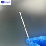
wafer lift pin sapphire lift pin&rod for wafer transfer Al2O3 material sapphire lift pin's Overview Sapphire Lift Pins are critical components used in ...
2025-05-06 20:40:03
|
|
... Substrates. It has a crystal structure of silicon carbide where the silicon and carbon atoms are arranged in a cubic lattice with a diamond-like ...
2025-05-06 20:41:43
|
|
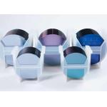
Semi-Insulating SiC Composite Substrates Epi ready 6inch 150mm for optoelectronic devices Summary for Semi-Insulating SiC Composite Substrates The ...
2025-05-06 20:41:34
|
|
...substrate Epitaxy 4inch 6inch 8inch for LED or Power device GaN-on-Si substrate abstract GaN-on-Si (111) substrates are essential in high...
2025-05-06 20:45:21
|
|
... used in material science and electronics research due to their versatile properties. Available in dimensions of 5x5x0.5 mm, 10x10x1 mm, and ...
2025-05-06 20:45:48
|
|
2inch/3inch/4inch S/Fe/Zn doped InP Indium Phosphide Single Crystal Wafer Indium phosphide (InP) is an important compound semiconductor material with ...
2025-05-06 20:44:34
|
|
.... SiC is used in semiconductor electronics devices that operate at high temperatures or high voltages, or both.SiC is also one of the important LED ...
2025-05-06 20:40:48
|