
191 - 200 of 281
dsp windows substrate wafer
Selling leads
|
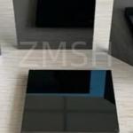
...-sized substrates that play a crucial role in various semiconductor applications. Commonly used in compact electronic devices where space is ...
2025-05-06 20:41:38
|

|
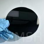
Si wafer 4inch Polished CZ Dopant Arsenic(As) Boron(B) Phosphorus(Ph) (100) Semiconductor Describe of Si Wafer: A Silicon wafer is a very thin round ...
2025-05-06 20:45:29
|
|
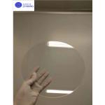
2inch 4inch 6inch 8inch 12inch Si wafer Silicon wafer Polishing Undoped P type N type Semiconductor Description of Si Wafer: Silicon wafer is a ...
2025-05-06 20:45:33
|
|
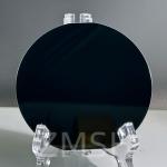
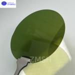
Fused Silica wafer JGS1 JGS2 BF33 8inch 12inch thickeness 750um±25um Ra ≤ 0.5nm TTV ≤ 10um Fused Silica wafer JGS1 JGS2 BF33 8inch 12inch‘s summary ...
2025-05-06 20:45:40
|
|
SOI Wafer Silicon-on-Insulator Wafer 4inch 5inch 6inch 8inch (100) (111) P Type N Type Description of SOI Wafer: SOI wafer refers to a thin layer of ...
2025-05-06 20:45:41
|
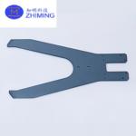
SiC Wafer Hand for Wafer Handling, Cleanroom Compatible, Corrosion Resistant, Customizable Interface
|
..., it offers excellent mechanical strength, corrosion resistance, thermal durability, and ultra-clean performance. It is ideal for handling advanced ...
2025-05-29 00:09:29
|
|
SiC Epitaxial Wafer Overview 4-inch (100 mm) SiC Epitaxial Wafers continue to play a vital role in the semiconductor market, serving as a highly ...
2025-07-10 18:23:23
|
|
... Substrate Indium Arsenide InAs wafer Application Indium Arsenide (InAs) single crystal semiconductor substrates are materials with unique ...
2025-07-19 00:11:40
|
|
N-type conductive SiC substrate composite substrate 6inch for Epitaxy MBE CVD LPE N-type conductive SiC substrate abstract This N-type conductive SiC ...
2025-05-06 20:41:32
|
|
Product Description: Our InP (Indium Phosphide) semiconductor wafers, renowned for their exceptional electronic and optoelectronic properties, have ...
2025-05-06 20:44:23
|